MC9S12NE64CPV Freescale Semiconductor, MC9S12NE64CPV Datasheet - Page 16
MC9S12NE64CPV
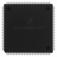
Manufacturer Part Number
MC9S12NE64CPV
Description
IC MCU 25MHZ ETHERNT/PHY 112LQFP
Manufacturer
Freescale Semiconductor
Series
HCS12r
Datasheet
1.MC9S12NE64VTU.pdf
(554 pages)
Specifications of MC9S12NE64CPV
Mfg Application Notes
MC9S12NE64 Integrated Ethernet Controller Implementing an Ethernet Interface with the MC9S12NE64 Web Server Development with MC9S12NE64 and Open TCP
Core Processor
HCS12
Core Size
16-Bit
Speed
25MHz
Connectivity
EBI/EMI, Ethernet, I²C, SCI, SPI
Peripherals
POR, PWM, WDT
Number Of I /o
70
Program Memory Size
64KB (64K x 8)
Program Memory Type
FLASH
Ram Size
8K x 8
Voltage - Supply (vcc/vdd)
2.375 V ~ 3.465 V
Data Converters
A/D 8x10b
Oscillator Type
Internal
Operating Temperature
-40°C ~ 85°C
Package / Case
112-LQFP
Data Bus Width
16 bit
Data Ram Size
8 KB
Interface Type
I2C, SCI, SPI
Maximum Clock Frequency
25 MHz
Number Of Programmable I/os
70
Number Of Timers
16 bit
Operating Supply Voltage
- 0.3 V to + 3 V
Maximum Operating Temperature
+ 105 C
Mounting Style
SMD/SMT
Minimum Operating Temperature
- 65 C
On-chip Adc
10 bit
For Use With
EVB9S12NE64E - BOARD EVAL FOR 9S12NE64DEMO9S12NE64E - DEMO BOARD FOR 9S12NE64
Lead Free Status / RoHS Status
Contains lead / RoHS non-compliant
Eeprom Size
-
Lead Free Status / Rohs Status
No RoHS Version Available
Available stocks
Company
Part Number
Manufacturer
Quantity
Price
Company:

Part Number:
MC9S12NE64CPV
Manufacturer:
RENESAS
Quantity:
21 000
Company:
Part Number:
MC9S12NE64CPV
Manufacturer:
FREESCAL
Quantity:
455
Company:
Part Number:
MC9S12NE64CPV
Manufacturer:
Freescale Semiconductor
Quantity:
10 000
Company:
Part Number:
MC9S12NE64CPVE
Manufacturer:
ST
Quantity:
445
Company:
Part Number:
MC9S12NE64CPVE
Manufacturer:
Freescale Semiconductor
Quantity:
10 000


17.1 Introduction . . . . . . . . . . . . . . . . . . . . . . . . . . . . . . . . . . . . . . . . . . . . . . . . . . . . . . . . . . . . . . . . . 443
17.2 External Signal Description . . . . . . . . . . . . . . . . . . . . . . . . . . . . . . . . . . . . . . . . . . . . . . . . . . . . . 444
17.3 Memory Map and Register Definition . . . . . . . . . . . . . . . . . . . . . . . . . . . . . . . . . . . . . . . . . . . . . 446
17.4 Functional Description . . . . . . . . . . . . . . . . . . . . . . . . . . . . . . . . . . . . . . . . . . . . . . . . . . . . . . . . . 452
18.1 Introduction . . . . . . . . . . . . . . . . . . . . . . . . . . . . . . . . . . . . . . . . . . . . . . . . . . . . . . . . . . . . . . . . . 469
18.2 External Signal Description . . . . . . . . . . . . . . . . . . . . . . . . . . . . . . . . . . . . . . . . . . . . . . . . . . . . . 473
18.3 Memory Map and Register Definition . . . . . . . . . . . . . . . . . . . . . . . . . . . . . . . . . . . . . . . . . . . . . 474
18.4 Functional Description . . . . . . . . . . . . . . . . . . . . . . . . . . . . . . . . . . . . . . . . . . . . . . . . . . . . . . . . . 489
16
16.4.1 Bus Control . . . . . . . . . . . . . . . . . . . . . . . . . . . . . . . . . . . . . . . . . . . . . . . . . . . . . . . . . . 435
16.4.2 Address Decoding . . . . . . . . . . . . . . . . . . . . . . . . . . . . . . . . . . . . . . . . . . . . . . . . . . . . . 436
16.4.3 Memory Expansion . . . . . . . . . . . . . . . . . . . . . . . . . . . . . . . . . . . . . . . . . . . . . . . . . . . . 437
17.1.1 Features . . . . . . . . . . . . . . . . . . . . . . . . . . . . . . . . . . . . . . . . . . . . . . . . . . . . . . . . . . . . . 443
17.1.2 Modes of Operation . . . . . . . . . . . . . . . . . . . . . . . . . . . . . . . . . . . . . . . . . . . . . . . . . . . . 444
17.2.1 BKGD — Background Interface Pin . . . . . . . . . . . . . . . . . . . . . . . . . . . . . . . . . . . . . . . 445
17.2.2 TAGHI — High Byte Instruction Tagging Pin . . . . . . . . . . . . . . . . . . . . . . . . . . . . . . . 445
17.2.3 TAGLO — Low Byte Instruction Tagging Pin . . . . . . . . . . . . . . . . . . . . . . . . . . . . . . . 445
17.3.1 Module Memory Map . . . . . . . . . . . . . . . . . . . . . . . . . . . . . . . . . . . . . . . . . . . . . . . . . . 446
17.3.2 Register Descriptions . . . . . . . . . . . . . . . . . . . . . . . . . . . . . . . . . . . . . . . . . . . . . . . . . . . 447
17.4.1 Security . . . . . . . . . . . . . . . . . . . . . . . . . . . . . . . . . . . . . . . . . . . . . . . . . . . . . . . . . . . . . 452
17.4.2 Enabling and Activating BDM . . . . . . . . . . . . . . . . . . . . . . . . . . . . . . . . . . . . . . . . . . . 452
17.4.3 BDM Hardware Commands . . . . . . . . . . . . . . . . . . . . . . . . . . . . . . . . . . . . . . . . . . . . . 453
17.4.4 Standard BDM Firmware Commands . . . . . . . . . . . . . . . . . . . . . . . . . . . . . . . . . . . . . . 454
17.4.5 BDM Command Structure . . . . . . . . . . . . . . . . . . . . . . . . . . . . . . . . . . . . . . . . . . . . . . . 455
17.4.6 BDM Serial Interface . . . . . . . . . . . . . . . . . . . . . . . . . . . . . . . . . . . . . . . . . . . . . . . . . . . 457
17.4.7 Serial Interface Hardware Handshake Protocol . . . . . . . . . . . . . . . . . . . . . . . . . . . . . . . 460
17.4.8 Hardware Handshake Abort Procedure . . . . . . . . . . . . . . . . . . . . . . . . . . . . . . . . . . . . . 462
17.4.9 SYNC — Request Timed Reference Pulse . . . . . . . . . . . . . . . . . . . . . . . . . . . . . . . . . . 465
17.4.10Instruction Tracing . . . . . . . . . . . . . . . . . . . . . . . . . . . . . . . . . . . . . . . . . . . . . . . . . . . . . 465
17.4.11Instruction Tagging . . . . . . . . . . . . . . . . . . . . . . . . . . . . . . . . . . . . . . . . . . . . . . . . . . . . 466
17.4.12Serial Communication Time-Out . . . . . . . . . . . . . . . . . . . . . . . . . . . . . . . . . . . . . . . . . . 466
17.4.13Operation in Wait Mode . . . . . . . . . . . . . . . . . . . . . . . . . . . . . . . . . . . . . . . . . . . . . . . . . 467
17.4.14Operation in Stop Mode . . . . . . . . . . . . . . . . . . . . . . . . . . . . . . . . . . . . . . . . . . . . . . . . . 467
18.1.1 Features . . . . . . . . . . . . . . . . . . . . . . . . . . . . . . . . . . . . . . . . . . . . . . . . . . . . . . . . . . . . . 469
18.1.2 Modes of Operation . . . . . . . . . . . . . . . . . . . . . . . . . . . . . . . . . . . . . . . . . . . . . . . . . . . . 471
18.1.3 Block Diagram . . . . . . . . . . . . . . . . . . . . . . . . . . . . . . . . . . . . . . . . . . . . . . . . . . . . . . . . 471
18.3.1 Module Memory Map . . . . . . . . . . . . . . . . . . . . . . . . . . . . . . . . . . . . . . . . . . . . . . . . . . 474
18.3.2 Register Descriptions . . . . . . . . . . . . . . . . . . . . . . . . . . . . . . . . . . . . . . . . . . . . . . . . . . . 474
18.4.1 DBG Operating in BKP Mode . . . . . . . . . . . . . . . . . . . . . . . . . . . . . . . . . . . . . . . . . . . . 489
Background Debug Module (BDMV4)
Debug Module (DBGV1)
MC9S12NE64 Data Sheet, Rev. 1.1
Chapter 17
Chapter 18
Freescale Semiconductor
Related parts for MC9S12NE64CPV
Image
Part Number
Description
Manufacturer
Datasheet
Request
R

Part Number:
Description:
Manufacturer:
Freescale Semiconductor, Inc
Datasheet:
Part Number:
Description:
Manufacturer:
Freescale Semiconductor, Inc
Datasheet:
Part Number:
Description:
Manufacturer:
Freescale Semiconductor, Inc
Datasheet:
Part Number:
Description:
Manufacturer:
Freescale Semiconductor, Inc
Datasheet:
Part Number:
Description:
Manufacturer:
Freescale Semiconductor, Inc
Datasheet:
Part Number:
Description:
Manufacturer:
Freescale Semiconductor, Inc
Datasheet:
Part Number:
Description:
Manufacturer:
Freescale Semiconductor, Inc
Datasheet:
Part Number:
Description:
Manufacturer:
Freescale Semiconductor, Inc
Datasheet:
Part Number:
Description:
Manufacturer:
Freescale Semiconductor, Inc
Datasheet:
Part Number:
Description:
Manufacturer:
Freescale Semiconductor, Inc
Datasheet:
Part Number:
Description:
Manufacturer:
Freescale Semiconductor, Inc
Datasheet:
Part Number:
Description:
Manufacturer:
Freescale Semiconductor, Inc
Datasheet:
Part Number:
Description:
Manufacturer:
Freescale Semiconductor, Inc
Datasheet:
Part Number:
Description:
Manufacturer:
Freescale Semiconductor, Inc
Datasheet:
Part Number:
Description:
Manufacturer:
Freescale Semiconductor, Inc
Datasheet: