MC9S12NE64CPV Freescale Semiconductor, MC9S12NE64CPV Datasheet - Page 86
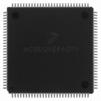
MC9S12NE64CPV
Manufacturer Part Number
MC9S12NE64CPV
Description
IC MCU 25MHZ ETHERNT/PHY 112LQFP
Manufacturer
Freescale Semiconductor
Series
HCS12r
Datasheet
1.MC9S12NE64VTU.pdf
(554 pages)
Specifications of MC9S12NE64CPV
Mfg Application Notes
MC9S12NE64 Integrated Ethernet Controller Implementing an Ethernet Interface with the MC9S12NE64 Web Server Development with MC9S12NE64 and Open TCP
Core Processor
HCS12
Core Size
16-Bit
Speed
25MHz
Connectivity
EBI/EMI, Ethernet, I²C, SCI, SPI
Peripherals
POR, PWM, WDT
Number Of I /o
70
Program Memory Size
64KB (64K x 8)
Program Memory Type
FLASH
Ram Size
8K x 8
Voltage - Supply (vcc/vdd)
2.375 V ~ 3.465 V
Data Converters
A/D 8x10b
Oscillator Type
Internal
Operating Temperature
-40°C ~ 85°C
Package / Case
112-LQFP
Data Bus Width
16 bit
Data Ram Size
8 KB
Interface Type
I2C, SCI, SPI
Maximum Clock Frequency
25 MHz
Number Of Programmable I/os
70
Number Of Timers
16 bit
Operating Supply Voltage
- 0.3 V to + 3 V
Maximum Operating Temperature
+ 105 C
Mounting Style
SMD/SMT
Minimum Operating Temperature
- 65 C
On-chip Adc
10 bit
For Use With
EVB9S12NE64E - BOARD EVAL FOR 9S12NE64DEMO9S12NE64E - DEMO BOARD FOR 9S12NE64
Lead Free Status / RoHS Status
Contains lead / RoHS non-compliant
Eeprom Size
-
Lead Free Status / Rohs Status
No RoHS Version Available
Available stocks
Company
Part Number
Manufacturer
Quantity
Price
Company:

Part Number:
MC9S12NE64CPV
Manufacturer:
RENESAS
Quantity:
21 000
Company:
Part Number:
MC9S12NE64CPV
Manufacturer:
FREESCAL
Quantity:
455
Company:
Part Number:
MC9S12NE64CPV
Manufacturer:
Freescale Semiconductor
Quantity:
10 000
Company:
Part Number:
MC9S12NE64CPVE
Manufacturer:
ST
Quantity:
445
Company:
Part Number:
MC9S12NE64CPVE
Manufacturer:
Freescale Semiconductor
Quantity:
10 000


Chapter 2 64 Kbyte Flash Module (S12FTS64KV3)
All bits read 0 and are not writable.
2.3.2.15
This register is reserved for factory testing and is not accessible.
All bits read 0 and are not writable.
2.4
2.4.1
Write and read operations are both used for the program, erase, erase verify, and data compress algorithms
described in this subsection. The program and erase algorithms are time controlled by a state machine
whose timebase, FCLK, is derived from the oscillator clock via a programmable divider. The command
register as well as the associated address and data registers operate as a buffer and a register (2-stage FIFO)
so that a second command along with the necessary data and address can be stored to the buffer while the
first command remains in progress. This pipelined operation allows a time optimization when
programming more than one word on a specific row in the Flash block as the high voltage generation can
be kept active in between two programming commands. The pipelined operation also allows a
simplification of command launching. Buffer empty as well as command completion are signalled by flags
in the Flash status register with interrupts generated, if enabled.
The next paragraphs describe:
86
Reset
Reset
1. How to write the FCLKDIV register.
2. Command write sequences used to program, erase, and verify the Flash memory.
3. Valid Flash commands.
4. Effects resulting from illegal Flash command write sequences or aborting Flash operations.
W
W
R
R
Functional Description
Flash Command Operations
RESERVED5
7
0
0
7
0
0
= Unimplemented or Reserved
= Unimplemented or Reserved
6
0
0
6
0
0
MC9S12NE64 Data Sheet, Rev. 1.1
5
0
0
5
0
0
Figure 2-19. RESERVED4
Figure 2-20. RESERVED5
4
0
0
4
0
0
3
0
0
3
0
0
2
0
0
2
0
0
Freescale Semiconductor
1
0
0
1
0
0
0
0
0
0
0
0
Related parts for MC9S12NE64CPV
Image
Part Number
Description
Manufacturer
Datasheet
Request
R

Part Number:
Description:
Manufacturer:
Freescale Semiconductor, Inc
Datasheet:
Part Number:
Description:
Manufacturer:
Freescale Semiconductor, Inc
Datasheet:
Part Number:
Description:
Manufacturer:
Freescale Semiconductor, Inc
Datasheet:
Part Number:
Description:
Manufacturer:
Freescale Semiconductor, Inc
Datasheet:
Part Number:
Description:
Manufacturer:
Freescale Semiconductor, Inc
Datasheet:
Part Number:
Description:
Manufacturer:
Freescale Semiconductor, Inc
Datasheet:
Part Number:
Description:
Manufacturer:
Freescale Semiconductor, Inc
Datasheet:
Part Number:
Description:
Manufacturer:
Freescale Semiconductor, Inc
Datasheet:
Part Number:
Description:
Manufacturer:
Freescale Semiconductor, Inc
Datasheet:
Part Number:
Description:
Manufacturer:
Freescale Semiconductor, Inc
Datasheet:
Part Number:
Description:
Manufacturer:
Freescale Semiconductor, Inc
Datasheet:
Part Number:
Description:
Manufacturer:
Freescale Semiconductor, Inc
Datasheet:
Part Number:
Description:
Manufacturer:
Freescale Semiconductor, Inc
Datasheet:
Part Number:
Description:
Manufacturer:
Freescale Semiconductor, Inc
Datasheet:
Part Number:
Description:
Manufacturer:
Freescale Semiconductor, Inc
Datasheet: