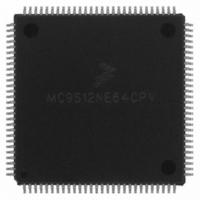
MC9S12NE64CPV Freescale Semiconductor, MC9S12NE64CPV Datasheet - Page 99

MC9S12NE64CPV
Manufacturer Part Number
MC9S12NE64CPV
Description
IC MCU 25MHZ ETHERNT/PHY 112LQFP
Manufacturer
Freescale Semiconductor
Series
HCS12r
Datasheet
1.MC9S12NE64VTU.pdf
(554 pages)
Specifications of MC9S12NE64CPV
Mfg Application Notes
MC9S12NE64 Integrated Ethernet Controller Implementing an Ethernet Interface with the MC9S12NE64 Web Server Development with MC9S12NE64 and Open TCP
Core Processor
HCS12
Core Size
16-Bit
Speed
25MHz
Connectivity
EBI/EMI, Ethernet, I²C, SCI, SPI
Peripherals
POR, PWM, WDT
Number Of I /o
70
Program Memory Size
64KB (64K x 8)
Program Memory Type
FLASH
Ram Size
8K x 8
Voltage - Supply (vcc/vdd)
2.375 V ~ 3.465 V
Data Converters
A/D 8x10b
Oscillator Type
Internal
Operating Temperature
-40°C ~ 85°C
Package / Case
112-LQFP
Data Bus Width
16 bit
Data Ram Size
8 KB
Interface Type
I2C, SCI, SPI
Maximum Clock Frequency
25 MHz
Number Of Programmable I/os
70
Number Of Timers
16 bit
Operating Supply Voltage
- 0.3 V to + 3 V
Maximum Operating Temperature
+ 105 C
Mounting Style
SMD/SMT
Minimum Operating Temperature
- 65 C
On-chip Adc
10 bit
For Use With
EVB9S12NE64E - BOARD EVAL FOR 9S12NE64DEMO9S12NE64E - DEMO BOARD FOR 9S12NE64
Lead Free Status / RoHS Status
Contains lead / RoHS non-compliant
Eeprom Size
-
Lead Free Status / Rohs Status
No RoHS Version Available
Available stocks
Company
Part Number
Manufacturer
Quantity
Price
Company:
Part Number:
MC9S12NE64CPV
Manufacturer:
RENESAS
Quantity:
21 000
Company:
Part Number:
MC9S12NE64CPV
Manufacturer:
FREESCAL
Quantity:
455
Company:
Part Number:
MC9S12NE64CPV
Manufacturer:
Freescale Semiconductor
Quantity:
10 000
Company:
Part Number:
MC9S12NE64CPVE
Manufacturer:
ST
Quantity:
445
Company:
Part Number:
MC9S12NE64CPVE
Manufacturer:
Freescale Semiconductor
Quantity:
10 000
- Current page: 99 of 554
- Download datasheet (4Mb)
2.4.1.4
The ACCERR flag will be set during the command write sequence if any of the following illegal steps are
performed, causing the command write sequence to immediately abort:
The ACCERR flag will not be set if any Flash register is read during a valid command write sequence.
The ACCERR flag will also be set if any of the following events occur:
If the Flash memory is read during execution of an algorithm (i.e., CCIF flag in the FSTAT register is low),
the read operation will return invalid data and the ACCERR flag will not be set.
If the ACCERR flag is set in the FSTAT register, the user must clear the ACCERR flag before starting
another command write sequence (see
The PVIOL flag will be set after the command is written to the FCMD register during a command write
sequence if any of the following illegal operations are attempted, causing the command write sequence to
immediately abort:
If the PVIOL flag is set in the FSTAT register, the user must clear the PVIOL flag before starting another
command write sequence (see
Freescale Semiconductor
1. Writing to a Flash address before initializing the FCLKDIV register.
2. Writing a byte or misaligned word to a valid Flash address.
3. Starting a command write sequence while a data compress operation is active.
4. Starting a command write sequence while a sector erase abort operation is active.
5. Writing a second word to a Flash address in the same command write sequence.
6. Writing to any Flash register other than FCMD after writing a word to a Flash address.
7. Writing a second command to the FCMD register in the same command write sequence.
8. Writing an invalid command to the FCMD register.
9. When security is enabled, writing a command other than mass erase to the FCMD register when
10. Writing to any Flash register other than FSTAT (to clear CBEIF) after writing to the FCMD
11. Writing a 0 to the CBEIF flag in the FSTAT register to abort a command write sequence.
1. Launching the sector erase abort command while a sector erase operation is active which results in
2. The MCU enters stop mode and a program or erase operation is in progress. The operation is
1. Writing the program command if the address written in the command write sequence was in a
2. Writing the sector erase command if the address written in the command write sequence was in a
3. Writing the mass erase command while any Flash protection is enabled.
the write originates from a non-secure memory location or from the Background Debug Mode.
register.
the early termination of the sector erase operation (see
Command”)
aborted immediately and any pending command is purged (see
protected area of the Flash memory.
protected area of the Flash memory.
Illegal Flash Operations
Section 2.3.2.7, “Flash Status Register
MC9S12NE64 Data Sheet, Rev. 1.1
Section 2.3.2.7, “Flash Status Register
Section 2.4.1.3.6, “Sector Erase Abort
(FSTAT)”).
Section 2.5.2, “Stop
(FSTAT)”).
Functional Description
Mode”).
99
Related parts for MC9S12NE64CPV
Image
Part Number
Description
Manufacturer
Datasheet
Request
R
Part Number:
Description:
Manufacturer:
Freescale Semiconductor, Inc
Datasheet:
Part Number:
Description:
Manufacturer:
Freescale Semiconductor, Inc
Datasheet:
Part Number:
Description:
Manufacturer:
Freescale Semiconductor, Inc
Datasheet:
Part Number:
Description:
Manufacturer:
Freescale Semiconductor, Inc
Datasheet:
Part Number:
Description:
Manufacturer:
Freescale Semiconductor, Inc
Datasheet:
Part Number:
Description:
Manufacturer:
Freescale Semiconductor, Inc
Datasheet:
Part Number:
Description:
Manufacturer:
Freescale Semiconductor, Inc
Datasheet:
Part Number:
Description:
Manufacturer:
Freescale Semiconductor, Inc
Datasheet:
Part Number:
Description:
Manufacturer:
Freescale Semiconductor, Inc
Datasheet:
Part Number:
Description:
Manufacturer:
Freescale Semiconductor, Inc
Datasheet:
Part Number:
Description:
Manufacturer:
Freescale Semiconductor, Inc
Datasheet:
Part Number:
Description:
Manufacturer:
Freescale Semiconductor, Inc
Datasheet:
Part Number:
Description:
Manufacturer:
Freescale Semiconductor, Inc
Datasheet:
Part Number:
Description:
Manufacturer:
Freescale Semiconductor, Inc
Datasheet:
Part Number:
Description:
Manufacturer:
Freescale Semiconductor, Inc
Datasheet:


