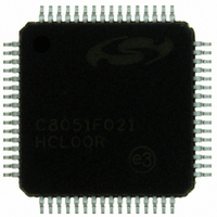
C8051F021-GQ Silicon Laboratories Inc, C8051F021-GQ Datasheet - Page 148

C8051F021-GQ
Manufacturer Part Number
C8051F021-GQ
Description
IC 8051 MCU 64K FLASH 64TQFP
Manufacturer
Silicon Laboratories Inc
Series
C8051F02xr
Specifications of C8051F021-GQ
Program Memory Type
FLASH
Program Memory Size
64KB (64K x 8)
Package / Case
64-TQFP, 64-VQFP
Core Processor
8051
Core Size
8-Bit
Speed
25MHz
Connectivity
EBI/EMI, SMBus (2-Wire/I²C), SPI, UART/USART
Peripherals
Brown-out Detect/Reset, POR, PWM, Temp Sensor, WDT
Number Of I /o
32
Ram Size
4.25K x 8
Voltage - Supply (vcc/vdd)
2.7 V ~ 3.6 V
Data Converters
A/D 8x8b, 8x12b; D/A 2x12b
Oscillator Type
Internal
Operating Temperature
-40°C ~ 85°C
Processor Series
C8051F0x
Core
8051
Data Bus Width
8 bit
Data Ram Size
4.25 KB
Interface Type
I2C/SMBus/SPI/UART
Maximum Clock Frequency
25 MHz
Number Of Programmable I/os
32
Number Of Timers
4
Operating Supply Voltage
2.7 V to 3.6 V
Maximum Operating Temperature
+ 85 C
Mounting Style
SMD/SMT
3rd Party Development Tools
PK51, CA51, A51, ULINK2
Development Tools By Supplier
C8051F020DK
Minimum Operating Temperature
- 40 C
On-chip Adc
8-ch x 8-bit or 8-ch x 12-bit
On-chip Dac
2-ch x 12-bit
No. Of I/o's
32
Ram Memory Size
4352Byte
Cpu Speed
25MHz
No. Of Timers
5
No. Of Pwm Channels
5
Rohs Compliant
Yes
Data Rom Size
64 KB
A/d Bit Size
12 bit
A/d Channels Available
8
Height
1.05 mm
Length
10 mm
Supply Voltage (max)
3.6 V
Supply Voltage (min)
2.7 V
Width
10 mm
Lead Free Status / RoHS Status
Lead free / RoHS Compliant
For Use With
336-1200 - DEV KIT FOR F020/F021/F022/F023
Eeprom Size
-
Lead Free Status / Rohs Status
Lead free / RoHS Compliant
Other names
336-1201
Available stocks
Company
Part Number
Manufacturer
Quantity
Price
Company:
Part Number:
C8051F021-GQ
Manufacturer:
Silicon Laboratories Inc
Quantity:
10 000
Company:
Part Number:
C8051F021-GQR
Manufacturer:
SiliconL
Quantity:
2 000
Company:
Part Number:
C8051F021-GQR
Manufacturer:
Silicon Laboratories Inc
Quantity:
10 000
Part Number:
C8051F021-GQR
Manufacturer:
SILICON LABS/芯科
Quantity:
20 000
C8051F020/1/2/3
16.4. Multiplexed and Non-multiplexed Selection
The External Memory Interface is capable of acting in a Multiplexed mode or a Non-multiplexed mode, depending
on the state of the EMD2 (EMI0CF.4) bit.
16.4.1. Multiplexed Configuration
In Multiplexed mode, the Data Bus and the lower 8-bits of the Address Bus share the same Port pins: AD[7:0]. In this
mode, an external latch (74HC373 or equivalent logic gate) is used to hold the lower 8-bits of the RAM address. The
external latch is controlled by the ALE (Address Latch Enable) signal, which is driven by the External Memory Inter-
face logic. An example of a Multiplexed Configuration is shown in Figure 16.3.
In Multiplexed mode, the external MOVX operation can be broken into two phases delineated by the state of the ALE
signal. During the first phase, ALE is high and the lower 8-bits of the Address Bus are presented to AD[7:0]. During
this phase, the address latch is configured such that the ‘Q’ outputs reflect the states of the ‘D’ inputs. When ALE
falls, signaling the beginning of the second phase, the address latch outputs remain fixed and are no longer dependent
on the latch inputs. Later in the second phase, the Data Bus controls the state of the AD[7:0] port at the time /RD or
/WR is asserted.
See
148
E
M
I
F
Section “16.6.2. Multiplexed Mode” on page 156
AD[7:0]
A[15:8]
/WR
ALE
/RD
Figure 16.3. Multiplexed Configuration Example
ADDRESS/DATA BUS
ADDRESS BUS
Rev. 1.4
for more information.
V
DD
8
G
D
74HC373
Q
CE
A[15:8]
A[7:0]
I/O[7:0]
WE
OE
64K X 8
SRAM


