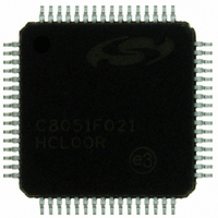
C8051F021-GQ Silicon Laboratories Inc, C8051F021-GQ Datasheet - Page 198

C8051F021-GQ
Manufacturer Part Number
C8051F021-GQ
Description
IC 8051 MCU 64K FLASH 64TQFP
Manufacturer
Silicon Laboratories Inc
Series
C8051F02xr
Specifications of C8051F021-GQ
Program Memory Type
FLASH
Program Memory Size
64KB (64K x 8)
Package / Case
64-TQFP, 64-VQFP
Core Processor
8051
Core Size
8-Bit
Speed
25MHz
Connectivity
EBI/EMI, SMBus (2-Wire/I²C), SPI, UART/USART
Peripherals
Brown-out Detect/Reset, POR, PWM, Temp Sensor, WDT
Number Of I /o
32
Ram Size
4.25K x 8
Voltage - Supply (vcc/vdd)
2.7 V ~ 3.6 V
Data Converters
A/D 8x8b, 8x12b; D/A 2x12b
Oscillator Type
Internal
Operating Temperature
-40°C ~ 85°C
Processor Series
C8051F0x
Core
8051
Data Bus Width
8 bit
Data Ram Size
4.25 KB
Interface Type
I2C/SMBus/SPI/UART
Maximum Clock Frequency
25 MHz
Number Of Programmable I/os
32
Number Of Timers
4
Operating Supply Voltage
2.7 V to 3.6 V
Maximum Operating Temperature
+ 85 C
Mounting Style
SMD/SMT
3rd Party Development Tools
PK51, CA51, A51, ULINK2
Development Tools By Supplier
C8051F020DK
Minimum Operating Temperature
- 40 C
On-chip Adc
8-ch x 8-bit or 8-ch x 12-bit
On-chip Dac
2-ch x 12-bit
No. Of I/o's
32
Ram Memory Size
4352Byte
Cpu Speed
25MHz
No. Of Timers
5
No. Of Pwm Channels
5
Rohs Compliant
Yes
Data Rom Size
64 KB
A/d Bit Size
12 bit
A/d Channels Available
8
Height
1.05 mm
Length
10 mm
Supply Voltage (max)
3.6 V
Supply Voltage (min)
2.7 V
Width
10 mm
Lead Free Status / RoHS Status
Lead free / RoHS Compliant
For Use With
336-1200 - DEV KIT FOR F020/F021/F022/F023
Eeprom Size
-
Lead Free Status / Rohs Status
Lead free / RoHS Compliant
Other names
336-1201
Available stocks
Company
Part Number
Manufacturer
Quantity
Price
Company:
Part Number:
C8051F021-GQ
Manufacturer:
Silicon Laboratories Inc
Quantity:
10 000
Company:
Part Number:
C8051F021-GQR
Manufacturer:
SiliconL
Quantity:
2 000
Company:
Part Number:
C8051F021-GQR
Manufacturer:
Silicon Laboratories Inc
Quantity:
10 000
Part Number:
C8051F021-GQR
Manufacturer:
SILICON LABS/芯科
Quantity:
20 000
C8051F020/1/2/3
19.1. Signal Descriptions
The four signals used by SPI0 (MOSI, MISO, SCK, NSS) are described below.
19.1.1. Master Out, Slave In (MOSI)
The master-out, slave-in (MOSI) signal is an output from a master device and an input to slave devices. It is used to
serially transfer data from the master to the slave. This signal is an output when SPI0 is operating as a master, and an
input when SPI0 is operating as a slave. Data is transferred most-significant bit first.
19.1.2. Master In, Slave Out (MISO)
The master-in, slave-out (MISO) signal is an output from a slave device and an input to the master device. It is used
to serially transfer data from the slave to the master. This signal is an input when SPI0 is operating as a master, and an
output when SPI0 is operating as a slave. Data is transferred most-significant bit first. A SPI slave places the MISO
pin in a high-impedance state when the slave is not selected.
19.1.3. Serial Clock (SCK)
The serial clock (SCK) signal is an output from the master device and an input to slave devices. It is used to synchro-
nize the transfer of data between the master and slave on the MOSI and MISO lines. SPI0 generates this signal when
operating as a master.
19.1.4. Slave Select (NSS)
The slave select (NSS) signal is an input used to select SPI0 as a slave, or to disable SPI0 as a master. Note that the
NSS signal is always an input to SPI0; with SPI0 operating as a master, slave select signals must be output via general
purpose port I/O pins. See Figure 19.2 for a typical configuration; see Section
ority Crossbar
The NSS signal must be low to initiate a transfer with SPI0 as a slave; SPI0 will exit slave mode when NSS is
released high. Note that received data is not latched into the receive buffer until NSS is high. For multiple-byte trans-
fers, NSS must be released high for at least 4 system clocks following each byte that is received by the SPI0 slave.
198
Decoder” on page
Master
Device
GPIO
MISO
MOSI
SCK
Figure 19.2. Typical SPI Interconnection
163
for general purpose port configuration.
Device
Slave
NSS
Rev. 1.4
Device
Slave
NSS
Device
“17.1. Ports 0 through 3 and the Pri-
Slave
NSS
VDD
MISO
MOSI
SCK


