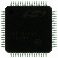
C8051F021-GQ Silicon Laboratories Inc, C8051F021-GQ Datasheet - Page 164

C8051F021-GQ
Manufacturer Part Number
C8051F021-GQ
Description
IC 8051 MCU 64K FLASH 64TQFP
Manufacturer
Silicon Laboratories Inc
Series
C8051F02xr
Specifications of C8051F021-GQ
Program Memory Type
FLASH
Program Memory Size
64KB (64K x 8)
Package / Case
64-TQFP, 64-VQFP
Core Processor
8051
Core Size
8-Bit
Speed
25MHz
Connectivity
EBI/EMI, SMBus (2-Wire/I²C), SPI, UART/USART
Peripherals
Brown-out Detect/Reset, POR, PWM, Temp Sensor, WDT
Number Of I /o
32
Ram Size
4.25K x 8
Voltage - Supply (vcc/vdd)
2.7 V ~ 3.6 V
Data Converters
A/D 8x8b, 8x12b; D/A 2x12b
Oscillator Type
Internal
Operating Temperature
-40°C ~ 85°C
Processor Series
C8051F0x
Core
8051
Data Bus Width
8 bit
Data Ram Size
4.25 KB
Interface Type
I2C/SMBus/SPI/UART
Maximum Clock Frequency
25 MHz
Number Of Programmable I/os
32
Number Of Timers
4
Operating Supply Voltage
2.7 V to 3.6 V
Maximum Operating Temperature
+ 85 C
Mounting Style
SMD/SMT
3rd Party Development Tools
PK51, CA51, A51, ULINK2
Development Tools By Supplier
C8051F020DK
Minimum Operating Temperature
- 40 C
On-chip Adc
8-ch x 8-bit or 8-ch x 12-bit
On-chip Dac
2-ch x 12-bit
No. Of I/o's
32
Ram Memory Size
4352Byte
Cpu Speed
25MHz
No. Of Timers
5
No. Of Pwm Channels
5
Rohs Compliant
Yes
Data Rom Size
64 KB
A/d Bit Size
12 bit
A/d Channels Available
8
Height
1.05 mm
Length
10 mm
Supply Voltage (max)
3.6 V
Supply Voltage (min)
2.7 V
Width
10 mm
Lead Free Status / RoHS Status
Lead free / RoHS Compliant
For Use With
336-1200 - DEV KIT FOR F020/F021/F022/F023
Eeprom Size
-
Lead Free Status / Rohs Status
Lead free / RoHS Compliant
Other names
336-1201
Available stocks
Company
Part Number
Manufacturer
Quantity
Price
Company:
Part Number:
C8051F021-GQ
Manufacturer:
Silicon Laboratories Inc
Quantity:
10 000
Company:
Part Number:
C8051F021-GQR
Manufacturer:
SiliconL
Quantity:
2 000
Company:
Part Number:
C8051F021-GQR
Manufacturer:
Silicon Laboratories Inc
Quantity:
10 000
Part Number:
C8051F021-GQR
Manufacturer:
SILICON LABS/芯科
Quantity:
20 000
C8051F020/1/2/3
to a Port pin without assigning RX0 as well. Each combination of enabled peripherals results in a unique device pin-
out.
All Port pins on Ports 0 through 3 that are not allocated by the Crossbar can be accessed as General-Purpose I/O
(GPIO) pins by reading and writing the associated Port Data registers (See Figure 17.10, Figure 17.12, Figure 17.15,
and Figure 17.17), a set of SFRs which are both byte- and bit-addressable. The output states of Port pins that are allo-
cated by the Crossbar are controlled by the digital peripheral that is mapped to those pins. Writes to the Port Data reg-
isters (or associated Port bits) will have no effect on the states of these pins.
A Read of a Port Data register (or Port bit) will always return the logic state present at the pin itself, regardless of
whether the Crossbar has allocated the pin for peripheral use or not. An exception to this occurs during the execution
of a read-modify-write instruction (ANL, ORL, XRL, CPL, INC, DEC, DJNZ, JBC, CLR, SET, and the bitwise MOV
operation). During the read cycle of the read-modify-write instruction, it is the contents of the Port Data register, not
the state of the Port pins themselves, which is read.
Because the Crossbar registers affect the pinout of the peripherals of the device, they are typically configured in the
initialization code of the system before the peripherals themselves are configured. Once configured, the Crossbar reg-
isters are typically left alone.
Once the Crossbar registers have been properly configured, the Crossbar is enabled by setting XBARE (XBR2.6) to a
logic 1. Until XBARE is set to a logic 1, the output drivers on Ports 0 through 3 are explicitly disabled in order
to prevent possible contention on the Port pins while the Crossbar registers and other registers which can
affect the device pinout are being written.
The output drivers on Crossbar-assigned input signals (like RX0, for example) are explicitly disabled; thus the values
of the Port Data registers and the PnMDOUT registers have no effect on the states of these pins.
17.1.2. Configuring the Output Modes of the Port Pins
The output drivers on Ports 0 through 3 remain disabled until the Crossbar is enabled by setting XBARE (XBR2.6) to
a logic 1.
The output mode of each port pin can be configured as either Open-Drain or Push-Pull; the default state is Open-
Drain. In the Push-Pull configuration, writing a logic 0 to the associated bit in the Port Data register will cause the
Port pin to be driven to GND, and writing a logic 1 will cause the Port pin to be driven to VDD. In the Open-Drain
configuration, writing a logic 0 to the associated bit in the Port Data register will cause the Port pin to be driven to
GND, and a logic 1 will cause the Port pin to assume a high-impedance state. The Open-Drain configuration is useful
to prevent contention between devices in systems where the Port pin participates in a shared interconnection in which
multiple outputs are connected to the same physical wire (like the SDA signal on an SMBus connection).
The output modes of the Port pins on Ports 0 through 3 are determined by the bits in the associated PnMDOUT regis-
ters (See Figure 17.11, Figure 17.14, Figure 17.16, and Figure 17.18). For example, a logic 1 in P3MDOUT.7 will
configure the output mode of P3.7 to Push-Pull; a logic 0 in P3MDOUT.7 will configure the output mode of P3.7 to
Open-Drain. All Port pins default to Open-Drain output.
The PnMDOUT registers control the output modes of the port pins regardless of whether the Crossbar has allocated
the Port pin for a digital peripheral or not. The exceptions to this rule are: the Port pins connected to SDA, SCL, RX0
(if UART0 is in Mode 0), and RX1 (if UART1 is in Mode 0) are always configured as Open-Drain outputs, regardless
of the settings of the associated bits in the PnMDOUT registers.
164
Rev. 1.4


