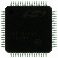
C8051F021-GQ Silicon Laboratories Inc, C8051F021-GQ Datasheet - Page 227

C8051F021-GQ
Manufacturer Part Number
C8051F021-GQ
Description
IC 8051 MCU 64K FLASH 64TQFP
Manufacturer
Silicon Laboratories Inc
Series
C8051F02xr
Specifications of C8051F021-GQ
Program Memory Type
FLASH
Program Memory Size
64KB (64K x 8)
Package / Case
64-TQFP, 64-VQFP
Core Processor
8051
Core Size
8-Bit
Speed
25MHz
Connectivity
EBI/EMI, SMBus (2-Wire/I²C), SPI, UART/USART
Peripherals
Brown-out Detect/Reset, POR, PWM, Temp Sensor, WDT
Number Of I /o
32
Ram Size
4.25K x 8
Voltage - Supply (vcc/vdd)
2.7 V ~ 3.6 V
Data Converters
A/D 8x8b, 8x12b; D/A 2x12b
Oscillator Type
Internal
Operating Temperature
-40°C ~ 85°C
Processor Series
C8051F0x
Core
8051
Data Bus Width
8 bit
Data Ram Size
4.25 KB
Interface Type
I2C/SMBus/SPI/UART
Maximum Clock Frequency
25 MHz
Number Of Programmable I/os
32
Number Of Timers
4
Operating Supply Voltage
2.7 V to 3.6 V
Maximum Operating Temperature
+ 85 C
Mounting Style
SMD/SMT
3rd Party Development Tools
PK51, CA51, A51, ULINK2
Development Tools By Supplier
C8051F020DK
Minimum Operating Temperature
- 40 C
On-chip Adc
8-ch x 8-bit or 8-ch x 12-bit
On-chip Dac
2-ch x 12-bit
No. Of I/o's
32
Ram Memory Size
4352Byte
Cpu Speed
25MHz
No. Of Timers
5
No. Of Pwm Channels
5
Rohs Compliant
Yes
Data Rom Size
64 KB
A/d Bit Size
12 bit
A/d Channels Available
8
Height
1.05 mm
Length
10 mm
Supply Voltage (max)
3.6 V
Supply Voltage (min)
2.7 V
Width
10 mm
Lead Free Status / RoHS Status
Lead free / RoHS Compliant
For Use With
336-1200 - DEV KIT FOR F020/F021/F022/F023
Eeprom Size
-
Lead Free Status / Rohs Status
Lead free / RoHS Compliant
Other names
336-1201
Available stocks
Company
Part Number
Manufacturer
Quantity
Price
Company:
Part Number:
C8051F021-GQ
Manufacturer:
Silicon Laboratories Inc
Quantity:
10 000
Company:
Part Number:
C8051F021-GQR
Manufacturer:
SiliconL
Quantity:
2 000
Company:
Part Number:
C8051F021-GQR
Manufacturer:
Silicon Laboratories Inc
Quantity:
10 000
Part Number:
C8051F021-GQR
Manufacturer:
SILICON LABS/芯科
Quantity:
20 000
22.1. Timer 0 and Timer 1
Timer 0 and Timer 1 are accessed and controlled through SFRs. Each counter/timer is implemented as a 16-bit regis-
ter accessed as two separate bytes: a low byte (TL0 or TL1) and a high byte (TH0 or TH1). The Counter/Timer Con-
trol (TCON) register is used to enable Timer 0 and Timer 1 as well as indicate their status. Both counter/timers
operate in one of four primary modes selected by setting the Mode Select bits M1-M0 in the Counter/Timer Mode
(TMOD) register. Each timer can be configured independently. Following is a detailed description of each operating
mode.
22.1.1. Mode 0: 13-bit Counter/Timer
Timer 0 and Timer 1 operate as a 13-bit counter/timer in Mode 0. The following describes the configuration and oper-
ation of Timer 0. However, both timers operate identically and Timer 1 is configured in the same manner as described
for Timer 0.
The TH0 register holds the eight MSBs of the 13-bit counter/timer. TL0 holds the five LSBs in bit positions TL0.4-
TL0.0. The three upper bits of TL0 (TL0.7-TL0.5) are indeterminate and should be masked out or ignored when read-
ing. As the 13-bit timer register increments and overflows from 0x1FFF (all ones) to 0x0000, the timer overflow flag
TF0 (TCON.5) is set and an interrupt will occur if enabled.
The C/T0 bit (TMOD.2) selects the counter/timer's clock source. Clearing C/T selects the system clock as the input
for the timer. When C/T0 is set to logic 1, high-to-low transitions at the selected input pin (T0) increment the timer
register. (Refer to
tion on selecting and configuring external I/O pins for digital peripherals.)
Setting the TR0 bit (TCON.4) enables the timer when either GATE0 (TMOD.3) is 0 or the input signal /INT0 is
logic-level one. Setting GATE0 to logic 1 allows the timer to be controlled by the external input signal /INT0, facili-
tating pulse width measurements.
Setting TR0 does not reset the timer register. The timer register should be initialized to the desired value before
enabling the timer.
TL1 and TH1 form the 13-bit register for Timer 1 in the same manner as described above for TL0 and TH0. Timer 1
is configured and controlled using the relevant TCON and TMOD bits just as with Timer 0.
TR0
X = Don't Care
0
1
1
1
GATE0
Section “17.1. Ports 0 through 3 and the Priority Crossbar Decoder” on page 163
X
0
1
1
/INT0
X
X
0
1
Counter/Timer
Disabled
Disabled
Enabled
Enabled
Rev. 1.4
C8051F020/1/2/3
for informa-
227


