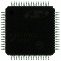
C8051F021-GQ Silicon Laboratories Inc, C8051F021-GQ Datasheet - Page 165

C8051F021-GQ
Manufacturer Part Number
C8051F021-GQ
Description
IC 8051 MCU 64K FLASH 64TQFP
Manufacturer
Silicon Laboratories Inc
Series
C8051F02xr
Specifications of C8051F021-GQ
Program Memory Type
FLASH
Program Memory Size
64KB (64K x 8)
Package / Case
64-TQFP, 64-VQFP
Core Processor
8051
Core Size
8-Bit
Speed
25MHz
Connectivity
EBI/EMI, SMBus (2-Wire/I²C), SPI, UART/USART
Peripherals
Brown-out Detect/Reset, POR, PWM, Temp Sensor, WDT
Number Of I /o
32
Ram Size
4.25K x 8
Voltage - Supply (vcc/vdd)
2.7 V ~ 3.6 V
Data Converters
A/D 8x8b, 8x12b; D/A 2x12b
Oscillator Type
Internal
Operating Temperature
-40°C ~ 85°C
Processor Series
C8051F0x
Core
8051
Data Bus Width
8 bit
Data Ram Size
4.25 KB
Interface Type
I2C/SMBus/SPI/UART
Maximum Clock Frequency
25 MHz
Number Of Programmable I/os
32
Number Of Timers
4
Operating Supply Voltage
2.7 V to 3.6 V
Maximum Operating Temperature
+ 85 C
Mounting Style
SMD/SMT
3rd Party Development Tools
PK51, CA51, A51, ULINK2
Development Tools By Supplier
C8051F020DK
Minimum Operating Temperature
- 40 C
On-chip Adc
8-ch x 8-bit or 8-ch x 12-bit
On-chip Dac
2-ch x 12-bit
No. Of I/o's
32
Ram Memory Size
4352Byte
Cpu Speed
25MHz
No. Of Timers
5
No. Of Pwm Channels
5
Rohs Compliant
Yes
Data Rom Size
64 KB
A/d Bit Size
12 bit
A/d Channels Available
8
Height
1.05 mm
Length
10 mm
Supply Voltage (max)
3.6 V
Supply Voltage (min)
2.7 V
Width
10 mm
Lead Free Status / RoHS Status
Lead free / RoHS Compliant
For Use With
336-1200 - DEV KIT FOR F020/F021/F022/F023
Eeprom Size
-
Lead Free Status / Rohs Status
Lead free / RoHS Compliant
Other names
336-1201
Available stocks
Company
Part Number
Manufacturer
Quantity
Price
Company:
Part Number:
C8051F021-GQ
Manufacturer:
Silicon Laboratories Inc
Quantity:
10 000
Company:
Part Number:
C8051F021-GQR
Manufacturer:
SiliconL
Quantity:
2 000
Company:
Part Number:
C8051F021-GQR
Manufacturer:
Silicon Laboratories Inc
Quantity:
10 000
Part Number:
C8051F021-GQR
Manufacturer:
SILICON LABS/芯科
Quantity:
20 000
17.1.3. Configuring Port Pins as Digital Inputs
A Port pin is configured as a digital input by setting its output mode to “Open-Drain” and writing a logic 1 to the
associated bit in the Port Data register. For example, P3.7 is configured as a digital input by setting P3MDOUT.7 to a
logic 0 and P3.7 to a logic 1.
If the Port pin has been assigned to a digital peripheral by the Crossbar and that pin functions as an input (for example
RX0, the UART0 receive pin), then the output drivers on that pin are automatically disabled.
17.1.4. External Interrupts (IE6 and IE7)
In addition to the external interrupts /INT0 and /INT1, whose Port pins are allocated and assigned by the Crossbar,
P3.6 and P3.7 can be configured to generate edge sensitive interrupts; these interrupts are configurable as falling- or
rising-edge sensitive using the IE6CF (P3IF.2) and IE7CF (P3IF.3) bits. When an active edge is detected on P3.6 or
P3.7, a corresponding External Interrupt flag (IE6 or IE7) will be set to a logic 1 in the P3IF register (See
Figure 17.19). If the associated interrupt is enabled, an interrupt will be generated and the CPU will vector to the
associated interrupt vector location. See
interrupts.
17.1.5. Weak Pull-ups
By default, each Port pin has an internal weak pull-up device enabled which provides a resistive connection (about
100 k) between the pin and VDD. The weak pull-up devices can be globally disabled by writing a logic 1 to the
Weak Pull-up Disable bit, (WEAKPUD, XBR2.7). The weak pull-up is automatically deactivated on any pin that is
driving a logic 0; that is, an output pin will not contend with its own pull-up device. The weak pull-up device can also
be explicitly disabled on a Port 1 pin by configuring the pin as an Analog Input, as described below.
17.1.6. Configuring Port 1 Pins as Analog Inputs (AIN1.[7:0])
The pins on Port 1 can serve as analog inputs to the ADC1 analog MUX. A Port pin is configured as an Analog Input
by writing a logic 0 to the associated bit in the P1MDIN register (see Figure 17.13). All Port pins default to a Digital
Input mode. Configuring a Port pin as an analog input:
Note that the output drivers on a pin configured as an Analog Input are not explicitly disabled. Therefore, the
associated P1MDOUT bits of pins configured as Analog Inputs should explicitly be set to logic 0 (Open-Drain output
mode), and the associated Port Data bits should be set to logic 1 (high-impedance). Also note that it is not required to
configure a Port pin as an Analog Input in order to use it as an input to the ADC1 MUX; however, it is strongly rec-
ommended. See
1.
2.
3.
Disables the digital input path from the pin. This prevents additional power supply current
from being drawn when the voltage at the pin is near VDD / 2. A read of the Port Data bit will
return a logic 0 regardless of the voltage at the Port pin.
Disables the weak pull-up device on the pin.
Causes the Crossbar to “skip over” the pin when allocating Port pins for digital peripherals.
Section “7. ADC1 (8-Bit ADC)” on page 75
Section “12.3. Interrupt Handler” on page 116
Rev. 1.4
for more information about ADC1.
C8051F020/1/2/3
for more information about
165


