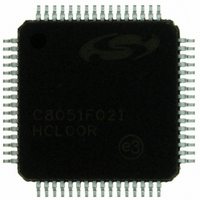
C8051F021-GQ Silicon Laboratories Inc, C8051F021-GQ Datasheet - Page 84

C8051F021-GQ
Manufacturer Part Number
C8051F021-GQ
Description
IC 8051 MCU 64K FLASH 64TQFP
Manufacturer
Silicon Laboratories Inc
Series
C8051F02xr
Specifications of C8051F021-GQ
Program Memory Type
FLASH
Program Memory Size
64KB (64K x 8)
Package / Case
64-TQFP, 64-VQFP
Core Processor
8051
Core Size
8-Bit
Speed
25MHz
Connectivity
EBI/EMI, SMBus (2-Wire/I²C), SPI, UART/USART
Peripherals
Brown-out Detect/Reset, POR, PWM, Temp Sensor, WDT
Number Of I /o
32
Ram Size
4.25K x 8
Voltage - Supply (vcc/vdd)
2.7 V ~ 3.6 V
Data Converters
A/D 8x8b, 8x12b; D/A 2x12b
Oscillator Type
Internal
Operating Temperature
-40°C ~ 85°C
Processor Series
C8051F0x
Core
8051
Data Bus Width
8 bit
Data Ram Size
4.25 KB
Interface Type
I2C/SMBus/SPI/UART
Maximum Clock Frequency
25 MHz
Number Of Programmable I/os
32
Number Of Timers
4
Operating Supply Voltage
2.7 V to 3.6 V
Maximum Operating Temperature
+ 85 C
Mounting Style
SMD/SMT
3rd Party Development Tools
PK51, CA51, A51, ULINK2
Development Tools By Supplier
C8051F020DK
Minimum Operating Temperature
- 40 C
On-chip Adc
8-ch x 8-bit or 8-ch x 12-bit
On-chip Dac
2-ch x 12-bit
No. Of I/o's
32
Ram Memory Size
4352Byte
Cpu Speed
25MHz
No. Of Timers
5
No. Of Pwm Channels
5
Rohs Compliant
Yes
Data Rom Size
64 KB
A/d Bit Size
12 bit
A/d Channels Available
8
Height
1.05 mm
Length
10 mm
Supply Voltage (max)
3.6 V
Supply Voltage (min)
2.7 V
Width
10 mm
Lead Free Status / RoHS Status
Lead free / RoHS Compliant
For Use With
336-1200 - DEV KIT FOR F020/F021/F022/F023
Eeprom Size
-
Lead Free Status / Rohs Status
Lead free / RoHS Compliant
Other names
336-1201
Available stocks
Company
Part Number
Manufacturer
Quantity
Price
Company:
Part Number:
C8051F021-GQ
Manufacturer:
Silicon Laboratories Inc
Quantity:
10 000
Company:
Part Number:
C8051F021-GQR
Manufacturer:
SiliconL
Quantity:
2 000
Company:
Part Number:
C8051F021-GQR
Manufacturer:
Silicon Laboratories Inc
Quantity:
10 000
Part Number:
C8051F021-GQR
Manufacturer:
SILICON LABS/芯科
Quantity:
20 000
C8051F020/1/2/3
8.1.1. Update Output On-Demand
In its default mode (DAC0CN.[4:3] = ‘00’) the DAC0 output is updated “on-demand” on a write to the high-byte of
the DAC0 data register (DAC0H). It’s important to note that writes to DAC0L are held, and have no effect on the
DAC0 output until a write to DAC0H takes place. If writing a full 12-bit word to the DAC data registers, the 12-bit
data word is written to the low byte (DAC0L) and high byte (DAC0H) data registers. Data is latched into DAC0 after
a write to the corresponding DAC0H register, so the write sequence should be DAC0L followed by DAC0H if the
full 12-bit resolution is required. The DAC can be used in 8-bit mode by initializing DAC0L to the desired value (typ-
ically 0x00), and writing data to only DAC0H (also see
Section 8.2
for information on formatting the 12-bit DAC
data word within the 16-bit SFR space).
8.1.2. Update Output Based on Timer Overflow
Similar to the ADC operation, in which an ADC conversion can be initiated by a timer overflow independently of the
processor, the DAC outputs can use a Timer overflow to schedule an output update event. This feature is useful in
systems where the DAC is used to generate a waveform of a defined sampling rate by eliminating the effects of vari-
able interrupt latency and instruction execution on the timing of the DAC output. When the DAC0MD bits
(DAC0CN.[4:3]) are set to ‘01’, ‘10’, or ‘11’, writes to both DAC data registers (DAC0L and DAC0H) are held until
an associated Timer overflow event (Timer 3, Timer 4, or Timer 2, respectively) occurs, at which time the
DAC0H:DAC0L contents are copied to the DAC input latches allowing the DAC output to change to the new value.
8.2.
DAC Output Scaling/Justification
In some instances, input data should be shifted prior to a DAC0 write operation to properly justify data within the
DAC input registers. This action would typically require one or more load and shift operations, adding software over-
head and slowing DAC throughput. To alleviate this problem, the data-formatting feature provides a means for the
user to program the orientation of the DAC0 data word within data registers DAC0H and DAC0L. The three
DAC0DF bits (DAC0CN.[2:0]) allow the user to specify one of five data word orientations as shown in the DAC0CN
register definition.
DAC1 is functionally the same as DAC0 described above. The electrical specifications for both DAC0 and DAC1 are
given in Table 8.1.
84
Rev. 1.4


