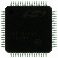
C8051F021-GQ Silicon Laboratories Inc, C8051F021-GQ Datasheet - Page 91

C8051F021-GQ
Manufacturer Part Number
C8051F021-GQ
Description
IC 8051 MCU 64K FLASH 64TQFP
Manufacturer
Silicon Laboratories Inc
Series
C8051F02xr
Specifications of C8051F021-GQ
Program Memory Type
FLASH
Program Memory Size
64KB (64K x 8)
Package / Case
64-TQFP, 64-VQFP
Core Processor
8051
Core Size
8-Bit
Speed
25MHz
Connectivity
EBI/EMI, SMBus (2-Wire/I²C), SPI, UART/USART
Peripherals
Brown-out Detect/Reset, POR, PWM, Temp Sensor, WDT
Number Of I /o
32
Ram Size
4.25K x 8
Voltage - Supply (vcc/vdd)
2.7 V ~ 3.6 V
Data Converters
A/D 8x8b, 8x12b; D/A 2x12b
Oscillator Type
Internal
Operating Temperature
-40°C ~ 85°C
Processor Series
C8051F0x
Core
8051
Data Bus Width
8 bit
Data Ram Size
4.25 KB
Interface Type
I2C/SMBus/SPI/UART
Maximum Clock Frequency
25 MHz
Number Of Programmable I/os
32
Number Of Timers
4
Operating Supply Voltage
2.7 V to 3.6 V
Maximum Operating Temperature
+ 85 C
Mounting Style
SMD/SMT
3rd Party Development Tools
PK51, CA51, A51, ULINK2
Development Tools By Supplier
C8051F020DK
Minimum Operating Temperature
- 40 C
On-chip Adc
8-ch x 8-bit or 8-ch x 12-bit
On-chip Dac
2-ch x 12-bit
No. Of I/o's
32
Ram Memory Size
4352Byte
Cpu Speed
25MHz
No. Of Timers
5
No. Of Pwm Channels
5
Rohs Compliant
Yes
Data Rom Size
64 KB
A/d Bit Size
12 bit
A/d Channels Available
8
Height
1.05 mm
Length
10 mm
Supply Voltage (max)
3.6 V
Supply Voltage (min)
2.7 V
Width
10 mm
Lead Free Status / RoHS Status
Lead free / RoHS Compliant
For Use With
336-1200 - DEV KIT FOR F020/F021/F022/F023
Eeprom Size
-
Lead Free Status / Rohs Status
Lead free / RoHS Compliant
Other names
336-1201
Available stocks
Company
Part Number
Manufacturer
Quantity
Price
Company:
Part Number:
C8051F021-GQ
Manufacturer:
Silicon Laboratories Inc
Quantity:
10 000
Company:
Part Number:
C8051F021-GQR
Manufacturer:
SiliconL
Quantity:
2 000
Company:
Part Number:
C8051F021-GQR
Manufacturer:
Silicon Laboratories Inc
Quantity:
10 000
Part Number:
C8051F021-GQR
Manufacturer:
SILICON LABS/芯科
Quantity:
20 000
9.
The voltage reference circuit offers full flexibility in operating the ADC and DAC modules. Three voltage reference
input pins allow each ADC and the two DACs to reference an external voltage reference or the on-chip voltage refer-
ence output. ADC0 may also reference the DAC0 output internally, and ADC1 may reference the analog power sup-
ply voltage, via the VREF multiplexers shown in Figure 9.1.
The internal voltage reference circuit consists of a 1.2 V, 15 ppm/°C (typical) bandgap voltage reference generator
and a gain-of-two output buffer amplifier. The internal reference may be routed via the VREF pin to external system
components or to the voltage reference input pins shown in Figure 9.1. Bypass capacitors of 0.1 µF and 4.7 µF are
recommended from the VREF pin to AGND, as shown in Figure 9.1. See Table 9.1 for voltage reference specifica-
tions.
The Reference Control Register, REF0CN (defined in Figure 9.2) enables/disables the internal reference generator
and selects the reference inputs for ADC0 and ADC1. The BIASE bit in REF0CN enables the on-board reference
generator while the REFBE bit enables the gain-of-two buffer amplifier which drives the VREF pin. When disabled,
the supply current drawn by the bandgap and buffer amplifier falls to less than 1 µA (typical) and the output of the
buffer amplifier enters a high impedance state. If the internal bandgap is used as the reference voltage generator,
BIASE and REFBE must both be set to logic 1. If the internal reference is not used, REFBE may be set to logic 0.
Note that the BIASE bit must be set to logic 1 if either DAC or ADC is used, regardless of whether the voltage refer-
ence is derived from the on-chip reference or supplied by an off-chip source. If neither the ADC nor the DAC are
being used, both of these bits can be set to logic 0 to conserve power. Bits AD0VRS and AD1VRS select the ADC0
and ADC1 voltage reference sources, respectively. The electrical specifications for the Voltage Reference circuit are
given in Table 9.1.
VOLTAGE REFERENCE (C8051F020/2)
Reference
External
Voltage
Circuit
Figure 9.1. Voltage Reference Functional Block Diagram
DGND
VDD
Recommended Bypass
4.7F
R1
Capacitors
0.1F
VREFD
VREF1
VREF0
VREF
Rev. 1.4
REF0CN
DAC0
DAC1
Ref
REFBE
x2
AV+
1
0
0
1
C8051F020/1/2/3
Band-Gap
BIASE
1.2V
EN
ADC1
ADC0
Ref
Ref
Bias to
ADCs,
DACs
91


