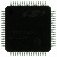
C8051F021-GQ Silicon Laboratories Inc, C8051F021-GQ Datasheet - Page 129

C8051F021-GQ
Manufacturer Part Number
C8051F021-GQ
Description
IC 8051 MCU 64K FLASH 64TQFP
Manufacturer
Silicon Laboratories Inc
Series
C8051F02xr
Specifications of C8051F021-GQ
Program Memory Type
FLASH
Program Memory Size
64KB (64K x 8)
Package / Case
64-TQFP, 64-VQFP
Core Processor
8051
Core Size
8-Bit
Speed
25MHz
Connectivity
EBI/EMI, SMBus (2-Wire/I²C), SPI, UART/USART
Peripherals
Brown-out Detect/Reset, POR, PWM, Temp Sensor, WDT
Number Of I /o
32
Ram Size
4.25K x 8
Voltage - Supply (vcc/vdd)
2.7 V ~ 3.6 V
Data Converters
A/D 8x8b, 8x12b; D/A 2x12b
Oscillator Type
Internal
Operating Temperature
-40°C ~ 85°C
Processor Series
C8051F0x
Core
8051
Data Bus Width
8 bit
Data Ram Size
4.25 KB
Interface Type
I2C/SMBus/SPI/UART
Maximum Clock Frequency
25 MHz
Number Of Programmable I/os
32
Number Of Timers
4
Operating Supply Voltage
2.7 V to 3.6 V
Maximum Operating Temperature
+ 85 C
Mounting Style
SMD/SMT
3rd Party Development Tools
PK51, CA51, A51, ULINK2
Development Tools By Supplier
C8051F020DK
Minimum Operating Temperature
- 40 C
On-chip Adc
8-ch x 8-bit or 8-ch x 12-bit
On-chip Dac
2-ch x 12-bit
No. Of I/o's
32
Ram Memory Size
4352Byte
Cpu Speed
25MHz
No. Of Timers
5
No. Of Pwm Channels
5
Rohs Compliant
Yes
Data Rom Size
64 KB
A/d Bit Size
12 bit
A/d Channels Available
8
Height
1.05 mm
Length
10 mm
Supply Voltage (max)
3.6 V
Supply Voltage (min)
2.7 V
Width
10 mm
Lead Free Status / RoHS Status
Lead free / RoHS Compliant
For Use With
336-1200 - DEV KIT FOR F020/F021/F022/F023
Eeprom Size
-
Lead Free Status / Rohs Status
Lead free / RoHS Compliant
Other names
336-1201
Available stocks
Company
Part Number
Manufacturer
Quantity
Price
Company:
Part Number:
C8051F021-GQ
Manufacturer:
Silicon Laboratories Inc
Quantity:
10 000
Company:
Part Number:
C8051F021-GQR
Manufacturer:
SiliconL
Quantity:
2 000
Company:
Part Number:
C8051F021-GQR
Manufacturer:
Silicon Laboratories Inc
Quantity:
10 000
Part Number:
C8051F021-GQR
Manufacturer:
SILICON LABS/芯科
Quantity:
20 000
C8051F020/1/2/3
13.3. External Reset
The external /RST pin provides a means for external circuitry to force the MCU into a reset state. Asserting the /RST
pin low will cause the MCU to enter the reset state. It may be desirable to provide an external pull-up and/or decou-
pling of the /RST pin to avoid erroneous noise-induced resets. The MCU will remain in reset until at least 12 clock
cycles after the active-low /RST signal is removed. The PINRSF flag (RSTSRC.0) is set on exit from an external
reset.
13.4. Software Forced Reset
Writing a ‘1’ to the SWRSEF bit forces a Software Reset as described in
Section
13.1.
13.5. Missing Clock Detector Reset
The Missing Clock Detector is essentially a one-shot circuit that is triggered by the MCU system clock. If the system
clock goes away for more than 100 µs, the one-shot will time out and generate a reset. After a Missing Clock Detector
reset, the MCDRSF flag (RSTSRC.2) will be set, signifying the MSD as the reset source; otherwise, this bit reads ‘0’.
The state of the /RST pin is unaffected by this reset. Setting the MSCLKE bit in the OSCICN register (see Section
“14.
OSCILLATORS” on page 135) enables the Missing Clock Detector.
13.6. Comparator0 Reset
Comparator0 can be configured as a reset input by writing a ‘1’ to the C0RSEF flag (RSTSRC.5). Comparator0
should be enabled using CPT0CN.7 (see Section
“11.
COMPARATORS” on page 95) prior to writing to C0RSEF to
prevent any turn-on chatter on the output from generating an unwanted reset. The Comparator0 reset is active-low: if
the non-inverting input voltage (CP0+ pin) is less than the inverting input voltage (CP0- pin), the MCU is put into the
reset state. After a Comparator0 Reset, the C0RSEF flag (RSTSRC.5) will read ‘1’ signifying Comparator0 as the
reset source; otherwise, this bit reads ‘0’. The state of the /RST pin is unaffected by this reset.
13.7. External CNVSTR Pin Reset
The external CNVSTR signal can be configured as a reset input by writing a ‘1’ to the CNVRSEF flag (RSTSRC.6).
The CNVSTR signal can appear on any of the P0, P1, P2 or P3 I/O pins as described in Section
“17.1. Ports 0
through 3 and the Priority Crossbar
Decoder” on page 163. Note that the Crossbar must be configured for the
CNVSTR signal to be routed to the appropriate Port I/O. The Crossbar should be configured and enabled before the
CNVRSEF is set. When configured as a reset, CNVSTR is active-low and level sensitive. After a CNVSTR reset, the
CNVRSEF flag (RSTSRC.6) will read ‘1’ signifying CNVSTR as the reset source; otherwise, this bit reads ‘0’. The
state of the /RST pin is unaffected by this reset.
13.8. Watchdog Timer Reset
The MCU includes a programmable Watchdog Timer (WDT) running off the system clock. A WDT overflow will
force the MCU into the reset state. To prevent the reset, the WDT must be restarted by application software before
overflow. If the system experiences a software/hardware malfunction preventing the software from restarting the
WDT, the WDT will overflow and cause a reset. This should prevent the system from running out of control.
Following a reset the WDT is automatically enabled and running with the default maximum time interval. If desired
the WDT can be disabled by system software or locked on to prevent accidental disabling. Once locked, the WDT
cannot be disabled until the next system reset. The state of the /RST pin is unaffected by this reset.
The WDT consists of a 21-bit timer running from the programmed system clock. The timer measures the period
between specific writes to its control register. If this period exceeds the programmed limit, a WDT reset is generated.
The WDT can be enabled and disabled as needed in software, or can be permanently enabled if desired. Watchdog
features are controlled via the Watchdog Timer Control Register (WDTCN) shown in Figure 13.3.
Rev. 1.4
129


