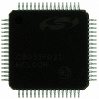
C8051F021-GQ Silicon Laboratories Inc, C8051F021-GQ Datasheet - Page 95

C8051F021-GQ
Manufacturer Part Number
C8051F021-GQ
Description
IC 8051 MCU 64K FLASH 64TQFP
Manufacturer
Silicon Laboratories Inc
Series
C8051F02xr
Specifications of C8051F021-GQ
Program Memory Type
FLASH
Program Memory Size
64KB (64K x 8)
Package / Case
64-TQFP, 64-VQFP
Core Processor
8051
Core Size
8-Bit
Speed
25MHz
Connectivity
EBI/EMI, SMBus (2-Wire/I²C), SPI, UART/USART
Peripherals
Brown-out Detect/Reset, POR, PWM, Temp Sensor, WDT
Number Of I /o
32
Ram Size
4.25K x 8
Voltage - Supply (vcc/vdd)
2.7 V ~ 3.6 V
Data Converters
A/D 8x8b, 8x12b; D/A 2x12b
Oscillator Type
Internal
Operating Temperature
-40°C ~ 85°C
Processor Series
C8051F0x
Core
8051
Data Bus Width
8 bit
Data Ram Size
4.25 KB
Interface Type
I2C/SMBus/SPI/UART
Maximum Clock Frequency
25 MHz
Number Of Programmable I/os
32
Number Of Timers
4
Operating Supply Voltage
2.7 V to 3.6 V
Maximum Operating Temperature
+ 85 C
Mounting Style
SMD/SMT
3rd Party Development Tools
PK51, CA51, A51, ULINK2
Development Tools By Supplier
C8051F020DK
Minimum Operating Temperature
- 40 C
On-chip Adc
8-ch x 8-bit or 8-ch x 12-bit
On-chip Dac
2-ch x 12-bit
No. Of I/o's
32
Ram Memory Size
4352Byte
Cpu Speed
25MHz
No. Of Timers
5
No. Of Pwm Channels
5
Rohs Compliant
Yes
Data Rom Size
64 KB
A/d Bit Size
12 bit
A/d Channels Available
8
Height
1.05 mm
Length
10 mm
Supply Voltage (max)
3.6 V
Supply Voltage (min)
2.7 V
Width
10 mm
Lead Free Status / RoHS Status
Lead free / RoHS Compliant
For Use With
336-1200 - DEV KIT FOR F020/F021/F022/F023
Eeprom Size
-
Lead Free Status / Rohs Status
Lead free / RoHS Compliant
Other names
336-1201
Available stocks
Company
Part Number
Manufacturer
Quantity
Price
Company:
Part Number:
C8051F021-GQ
Manufacturer:
Silicon Laboratories Inc
Quantity:
10 000
Company:
Part Number:
C8051F021-GQR
Manufacturer:
SiliconL
Quantity:
2 000
Company:
Part Number:
C8051F021-GQR
Manufacturer:
Silicon Laboratories Inc
Quantity:
10 000
Part Number:
C8051F021-GQR
Manufacturer:
SILICON LABS/芯科
Quantity:
20 000
11.
Each MCU includes two on-board voltage comparators as shown in Figure 11.1. The inputs of each Comparator are
available at the package pins. The output of each comparator is optionally available at the package pins via the I/O
crossbar. When assigned to package pins, each comparator output can be programmed to operate in open drain or
push-pull modes. See
details.
The hysteresis of each comparator is software-programmable via its respective Comparator control register (CPT0CN
and CPT1CN for Comparator0 and Comparator1, respectively). The user can program both the amount of hysteresis
voltage (referred to the input voltage) and the positive and negative-going symmetry of this hysteresis around the
threshold voltage. The output of the comparator can be polled in software, or can be used as an interrupt source. Each
comparator can be individually enabled or disabled (shutdown). When disabled, the comparator output (if assigned to
a Port I/O pin via the Crossbar) defaults to the logic low state, its interrupt capability is suspended and its supply cur-
rent falls to less than 1 µA. Comparator inputs can be externally driven from -0.25 V to (AV+) + 0.25 V without dam-
age or upset.
The Comparator0 hysteresis is programmed using bits 3-0 in the Comparator0 Control Register CPT0CN (shown in
Figure 11.1). The amount of negative hysteresis voltage is determined by the settings of the CP0HYN bits; In a simi-
lar way, the amount of positive hysteresis is determined by the setting the CP0HYP bits. See Table 11.1 on page 99
for hysteresis level specifications.
Comparator interrupts can be generated on rising-edge and/or falling-edge output transitions. (For interrupt enable
and priority control, see
Comparator0 falling-edge interrupt, and the CP0RIF flag is set upon the Comparator0 rising-edge interrupt. Once set,
these bits remain set until cleared by software. The Output State of Comparator0 can be obtained at any time by read-
ing the CP0OUT bit. Comparator0 is enabled by setting the CP0EN bit to logic 1, and is disabled by clearing this bit
COMPARATORS
CP0+
CP0-
CP1+
CP1-
Section “17. PORT INPUT/OUTPUT” on page 161
Figure 11.1. Comparator Functional Block Diagram
Section “12.3. Interrupt Handler” on page
CP0HYN1
CP0HYN0
CP1HYN1
CP1HYN0
CP0HYP1
CP0HYP0
CP1HYP1
CP1HYP0
CP0OUT
CP1OUT
CP0RIF
CP1RIF
CP0EN
CP0FIF
CP1EN
CP1FIF
Rev. 1.4
+
-
+
-
AV+
AV+
AGND
AGND
116). The CP0FIF flag is set upon a
Decision
(SYNCHRONIZER)
(SYNCHRONIZER)
Reset
D
D
Tree
SET
CLR
SET
CLR
Q
Q
Q
Q
for Crossbar and port initialization
C8051F020/1/2/3
D
D
SET
CLR
SET
CLR
Q
Q
Q
Q
Crossbar
Crossbar
Interrupt
Interrupt
Handler
Handler
95


