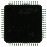
C8051F021-GQ Silicon Laboratories Inc, C8051F021-GQ Datasheet - Page 268

C8051F021-GQ
Manufacturer Part Number
C8051F021-GQ
Description
IC 8051 MCU 64K FLASH 64TQFP
Manufacturer
Silicon Laboratories Inc
Series
C8051F02xr
Specifications of C8051F021-GQ
Program Memory Type
FLASH
Program Memory Size
64KB (64K x 8)
Package / Case
64-TQFP, 64-VQFP
Core Processor
8051
Core Size
8-Bit
Speed
25MHz
Connectivity
EBI/EMI, SMBus (2-Wire/I²C), SPI, UART/USART
Peripherals
Brown-out Detect/Reset, POR, PWM, Temp Sensor, WDT
Number Of I /o
32
Ram Size
4.25K x 8
Voltage - Supply (vcc/vdd)
2.7 V ~ 3.6 V
Data Converters
A/D 8x8b, 8x12b; D/A 2x12b
Oscillator Type
Internal
Operating Temperature
-40°C ~ 85°C
Processor Series
C8051F0x
Core
8051
Data Bus Width
8 bit
Data Ram Size
4.25 KB
Interface Type
I2C/SMBus/SPI/UART
Maximum Clock Frequency
25 MHz
Number Of Programmable I/os
32
Number Of Timers
4
Operating Supply Voltage
2.7 V to 3.6 V
Maximum Operating Temperature
+ 85 C
Mounting Style
SMD/SMT
3rd Party Development Tools
PK51, CA51, A51, ULINK2
Development Tools By Supplier
C8051F020DK
Minimum Operating Temperature
- 40 C
On-chip Adc
8-ch x 8-bit or 8-ch x 12-bit
On-chip Dac
2-ch x 12-bit
No. Of I/o's
32
Ram Memory Size
4352Byte
Cpu Speed
25MHz
No. Of Timers
5
No. Of Pwm Channels
5
Rohs Compliant
Yes
Data Rom Size
64 KB
A/d Bit Size
12 bit
A/d Channels Available
8
Height
1.05 mm
Length
10 mm
Supply Voltage (max)
3.6 V
Supply Voltage (min)
2.7 V
Width
10 mm
Lead Free Status / RoHS Status
Lead free / RoHS Compliant
For Use With
336-1200 - DEV KIT FOR F020/F021/F022/F023
Eeprom Size
-
Lead Free Status / Rohs Status
Lead free / RoHS Compliant
Other names
336-1201
Available stocks
Company
Part Number
Manufacturer
Quantity
Price
Company:
Part Number:
C8051F021-GQ
Manufacturer:
Silicon Laboratories Inc
Quantity:
10 000
Company:
Part Number:
C8051F021-GQR
Manufacturer:
SiliconL
Quantity:
2 000
Company:
Part Number:
C8051F021-GQR
Manufacturer:
Silicon Laboratories Inc
Quantity:
10 000
Part Number:
C8051F021-GQR
Manufacturer:
SILICON LABS/芯科
Quantity:
20 000
C8051F020/1/2/3
24.2. Flash Programming Commands
The Flash memory can be programmed directly over the JTAG interface using the Flash Control, Flash Data, Flash
Address, and Flash Scale registers. These Indirect Data Registers are accessed via the JTAG Instruction Register.
Read and write operations on indirect data registers are performed by first setting the appropriate DR address in the
IR register. Each read or write is then initiated by writing the appropriate Indirect Operation Code (IndOpCode) to the
selected data register. Incoming commands to this register have the following format:
IndOpCode: These bit set the operation to perform according to the following table:
The Poll operation is used to check the Busy bit as described below. Although a Capture-DR is performed, no
Update-DR is allowed for the Poll operation. Since updates are disabled, polling can be accomplished by shifting in/
out a single bit.
The Read operation initiates a read from the register addressed by the DRAddress. Reads can be initiated by shifting
only 2 bits into the indirect register. After the read operation is initiated, polling of the Busy bit must be performed to
determine when the operation is complete.
The write operation initiates a write of WriteData to the register addressed by DRAddress. Registers of any width up
to 18 bits can be written. If the register to be written contains fewer than 18 bits, the data in WriteData should be left-
justified, i.e. its MSB should occupy bit 17 above. This allows shorter registers to be written in fewer JTAG clock
cycles. For example, an 8-bit register could be written by shifting only 10 bits. After a Write is initiated, the Busy bit
should be polled to determine when the next operation can be initiated. The contents of the Instruction Register
should not be altered while either a read or write operation is busy.
Outgoing data from the indirect Data Register has the following format:
The Busy bit indicates that the current operation is not complete. It goes high when an operation is initiated and
returns low when complete. Read and Write commands are ignored while Busy is high. In fact, if polling for Busy to
be low will be followed by another read or write operation, JTAG writes of the next operation can be made while
checking for Busy to be low. They will be ignored until Busy is read low, at which time the new operation will initi-
ate. This bit is placed ate bit 0 to allow polling by single-bit shifts. When waiting for a Read to complete and Busy is
0, the following 18 bits can be shifted out to obtain the resulting data. ReadData is always right-justified. This allows
registers shorter than 18 bits to be read using a reduced number of shifts. For example, the results from a byte-read
requires 9 bit shifts (Busy + 8 bits).
268
19
0
IndOpCode
19:18
IndOpCode
0x
10
11
ReadData
Rev. 1.4
18:1
Operation
WriteData
Write
Read
Poll
17:0
Busy
0


