C8051F021-GQ Silicon Laboratories Inc, C8051F021-GQ Datasheet - Page 269
C8051F021-GQ
Manufacturer Part Number
C8051F021-GQ
Description
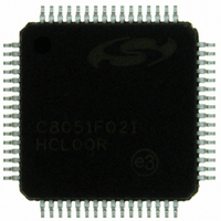
IC 8051 MCU 64K FLASH 64TQFP
Manufacturer
Silicon Laboratories Inc
Series
C8051F02xr
Specifications of C8051F021-GQ
Program Memory Type
FLASH
Program Memory Size
64KB (64K x 8)
Package / Case
64-TQFP, 64-VQFP
Core Processor
8051
Core Size
8-Bit
Speed
25MHz
Connectivity
EBI/EMI, SMBus (2-Wire/I²C), SPI, UART/USART
Peripherals
Brown-out Detect/Reset, POR, PWM, Temp Sensor, WDT
Number Of I /o
32
Ram Size
4.25K x 8
Voltage - Supply (vcc/vdd)
2.7 V ~ 3.6 V
Data Converters
A/D 8x8b, 8x12b; D/A 2x12b
Oscillator Type
Internal
Operating Temperature
-40°C ~ 85°C
Processor Series
C8051F0x
Core
8051
Data Bus Width
8 bit
Data Ram Size
4.25 KB
Interface Type
I2C/SMBus/SPI/UART
Maximum Clock Frequency
25 MHz
Number Of Programmable I/os
32
Number Of Timers
4
Operating Supply Voltage
2.7 V to 3.6 V
Maximum Operating Temperature
+ 85 C
Mounting Style
SMD/SMT
3rd Party Development Tools
PK51, CA51, A51, ULINK2
Development Tools By Supplier
C8051F020DK
Minimum Operating Temperature
- 40 C
On-chip Adc
8-ch x 8-bit or 8-ch x 12-bit
On-chip Dac
2-ch x 12-bit
No. Of I/o's
32
Ram Memory Size
4352Byte
Cpu Speed
25MHz
No. Of Timers
5
No. Of Pwm Channels
5
Rohs Compliant
Yes
Data Rom Size
64 KB
A/d Bit Size
12 bit
A/d Channels Available
8
Height
1.05 mm
Length
10 mm
Supply Voltage (max)
3.6 V
Supply Voltage (min)
2.7 V
Width
10 mm
Lead Free Status / RoHS Status
Lead free / RoHS Compliant
For Use With
336-1200 - DEV KIT FOR F020/F021/F022/F023
Eeprom Size
-
Lead Free Status / Rohs Status
Lead free / RoHS Compliant
Other names
336-1201
Available stocks
Company
Part Number
Manufacturer
Quantity
Price
Company:

Part Number:
C8051F021-GQ
Manufacturer:
Silicon Laboratories Inc
Quantity:
10 000
Company:
Part Number:
C8051F021-GQR
Manufacturer:
SiliconL
Quantity:
2 000
Company:
Part Number:
C8051F021-GQR
Manufacturer:
Silicon Laboratories Inc
Quantity:
10 000
Part Number:
C8051F021-GQR
Manufacturer:
SILICON LABS/芯科
Quantity:
20 000


This register determines how the Flash interface logic will respond to reads and writes to the FLASHDAT
Register.
Bit7:
Bits6-4:
Bits3-0:
SFLE
Bit7
SFLE: Scratchpad FLASH Memory Access Enable.
When this bit is set, FLASH reads and writes are directed to the 128-byte Scratchpad FLASH sector.
When SFLE is set to logic 1, FLASH accesses out of the address range 0x00-0x7F should not be
attempted. Reads/Writes out of this range will yield unpredictable results.
0:
1:
WRMD2-0: Write Mode Select Bits.
The Write Mode Select Bits control how the interface logic responds to writes to the FLASHDAT
Register per the following values:
000:
001:
010:
(All other values for WRMD3-0 are reserved.)
RDMD3-0: Read Mode Select Bits.
The Read Mode Select Bits control how the interface logic responds to reads to the FLASHDAT Reg-
ister per the following values:
0000:
0001:
0010:
(All other values for RDMD3-0 are reserved.)
WRMD2
Bit6
FLASH access directed to the 64k byte Program/Data FLASH sector.
FLASH access directed to the 128 byte Scratchpad sector.
A FLASHDAT write replaces the data in the FASHDAT register, but is otherwise ignored.
A FLASHDAT write initiates a write of FLASHDAT into the memory address by the
FLASHADR register. FLASHADR is incremented by one when complete.
A FLASHDAT write initiates an erasure (sets all bytes to 0xFF) of the Flash page containing
the address in FLASHADR. The data written must be 0xA5 for the erase to occur.
FLASHADR is not affected. If FLASHADR = 0x7DFE - 0x7DFF, the entire user space will
be erased (i.e. entire Flash memory except for Reserved area 0x7E00 - 0x7FFF).
A FLASHDAT read provides the data in the FASHDAT register, but is otherwise ignored.
A FLASHDAT read initiates a read of the byte addressed by the FLASHADR register if no
operation is currently active. This mode is used for block reads.
A FLASHDAT read initiates a read of the byte addressed by FLASHADR only if no
operation is active and any data from a previous read has already been read from
FLASHDAT. This mode allows single bytes to be read (or the last byte of a block) without
initiating an extra read.
Figure 24.3. FLASHCON: JTAG Flash Control Register
WRMD1
Bit5
WRMD0
Bit4
RDMD3
Bit3
Rev. 1.4
RDMD2
Bit2
RDMD1
C8051F020/1/2/3
Bit1
RDMD0
Bit0
00000000
Reset Value
269
Related parts for C8051F021-GQ
Image
Part Number
Description
Manufacturer
Datasheet
Request
R

Part Number:
Description:
SMD/C°/SINGLE-ENDED OUTPUT SILICON OSCILLATOR
Manufacturer:
Silicon Laboratories Inc
Part Number:
Description:
Manufacturer:
Silicon Laboratories Inc
Datasheet:
Part Number:
Description:
N/A N/A/SI4010 AES KEYFOB DEMO WITH LCD RX
Manufacturer:
Silicon Laboratories Inc
Datasheet:
Part Number:
Description:
N/A N/A/SI4010 SIMPLIFIED KEY FOB DEMO WITH LED RX
Manufacturer:
Silicon Laboratories Inc
Datasheet:
Part Number:
Description:
N/A/-40 TO 85 OC/EZLINK MODULE; F930/4432 HIGH BAND (REV E/B1)
Manufacturer:
Silicon Laboratories Inc
Part Number:
Description:
EZLink Module; F930/4432 Low Band (rev e/B1)
Manufacturer:
Silicon Laboratories Inc
Part Number:
Description:
I°/4460 10 DBM RADIO TEST CARD 434 MHZ
Manufacturer:
Silicon Laboratories Inc
Part Number:
Description:
I°/4461 14 DBM RADIO TEST CARD 868 MHZ
Manufacturer:
Silicon Laboratories Inc
Part Number:
Description:
I°/4463 20 DBM RFSWITCH RADIO TEST CARD 460 MHZ
Manufacturer:
Silicon Laboratories Inc
Part Number:
Description:
I°/4463 20 DBM RADIO TEST CARD 868 MHZ
Manufacturer:
Silicon Laboratories Inc
Part Number:
Description:
I°/4463 27 DBM RADIO TEST CARD 868 MHZ
Manufacturer:
Silicon Laboratories Inc
Part Number:
Description:
I°/4463 SKYWORKS 30 DBM RADIO TEST CARD 915 MHZ
Manufacturer:
Silicon Laboratories Inc
Part Number:
Description:
N/A N/A/-40 TO 85 OC/4463 RFMD 30 DBM RADIO TEST CARD 915 MHZ
Manufacturer:
Silicon Laboratories Inc
Part Number:
Description:
I°/4463 20 DBM RADIO TEST CARD 169 MHZ
Manufacturer:
Silicon Laboratories Inc