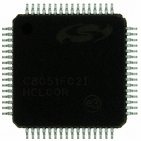
C8051F021-GQ Silicon Laboratories Inc, C8051F021-GQ Datasheet - Page 213

C8051F021-GQ
Manufacturer Part Number
C8051F021-GQ
Description
IC 8051 MCU 64K FLASH 64TQFP
Manufacturer
Silicon Laboratories Inc
Series
C8051F02xr
Specifications of C8051F021-GQ
Program Memory Type
FLASH
Program Memory Size
64KB (64K x 8)
Package / Case
64-TQFP, 64-VQFP
Core Processor
8051
Core Size
8-Bit
Speed
25MHz
Connectivity
EBI/EMI, SMBus (2-Wire/I²C), SPI, UART/USART
Peripherals
Brown-out Detect/Reset, POR, PWM, Temp Sensor, WDT
Number Of I /o
32
Ram Size
4.25K x 8
Voltage - Supply (vcc/vdd)
2.7 V ~ 3.6 V
Data Converters
A/D 8x8b, 8x12b; D/A 2x12b
Oscillator Type
Internal
Operating Temperature
-40°C ~ 85°C
Processor Series
C8051F0x
Core
8051
Data Bus Width
8 bit
Data Ram Size
4.25 KB
Interface Type
I2C/SMBus/SPI/UART
Maximum Clock Frequency
25 MHz
Number Of Programmable I/os
32
Number Of Timers
4
Operating Supply Voltage
2.7 V to 3.6 V
Maximum Operating Temperature
+ 85 C
Mounting Style
SMD/SMT
3rd Party Development Tools
PK51, CA51, A51, ULINK2
Development Tools By Supplier
C8051F020DK
Minimum Operating Temperature
- 40 C
On-chip Adc
8-ch x 8-bit or 8-ch x 12-bit
On-chip Dac
2-ch x 12-bit
No. Of I/o's
32
Ram Memory Size
4352Byte
Cpu Speed
25MHz
No. Of Timers
5
No. Of Pwm Channels
5
Rohs Compliant
Yes
Data Rom Size
64 KB
A/d Bit Size
12 bit
A/d Channels Available
8
Height
1.05 mm
Length
10 mm
Supply Voltage (max)
3.6 V
Supply Voltage (min)
2.7 V
Width
10 mm
Lead Free Status / RoHS Status
Lead free / RoHS Compliant
For Use With
336-1200 - DEV KIT FOR F020/F021/F022/F023
Eeprom Size
-
Lead Free Status / Rohs Status
Lead free / RoHS Compliant
Other names
336-1201
Available stocks
Company
Part Number
Manufacturer
Quantity
Price
Company:
Part Number:
C8051F021-GQ
Manufacturer:
Silicon Laboratories Inc
Quantity:
10 000
Company:
Part Number:
C8051F021-GQR
Manufacturer:
SiliconL
Quantity:
2 000
Company:
Part Number:
C8051F021-GQR
Manufacturer:
Silicon Laboratories Inc
Quantity:
10 000
Part Number:
C8051F021-GQR
Manufacturer:
SILICON LABS/芯科
Quantity:
20 000
Bits7-6:
Bit5:
Bit4:
Bit3:
Bit2:
Bit1:
Bit0:
SM00/FE0
R/W
Bit7
The function of these bits is determined by the SSTAT0 bit in register PCON.
If SSTAT0 is logic 1, these bits are UART0 status indicators as described in
If SSTAT0 is logic 0, these bits select the Serial Port Operation Mode as shown below.
SM00-SM10: Serial Port Operation Mode:
SM20: Multiprocessor Communication Enable.
If SSTAT0 is logic 1, this bit is a UART0 status indicator as described in
If SSTAT0 is logic 0, the function of this bit is dependent on the Serial Port Operation Mode.
Mode 0: No effect.
Mode 1: Checks for valid stop bit.
Modes 2 and 3: Multiprocessor Communications Enable.
REN0: Receive Enable.
This bit enables/disables the UART0 receiver.
0: UART0 reception disabled.
1: UART0 reception enabled.
TB80: Ninth Transmission Bit.
The logic level of this bit will be assigned to the ninth transmission bit in Modes 2 and 3. It is not used
in Modes 0 and 1. Set or cleared by software as required.
RB80: Ninth Receive Bit.
The bit is assigned the logic level of the ninth bit received in Modes 2 and 3. In Mode 1, if SM20 is
logic 0, RB80 is assigned the logic level of the received stop bit. RB8 is not used in Mode 0.
TI0: Transmit Interrupt Flag.
Set by hardware when a byte of data has been transmitted by UART0 (after the 8th bit in Mode 0, or
at the beginning of the stop bit in other modes). When the UART0 interrupt is enabled, setting this bit
causes the CPU to vector to the UART0 interrupt service routine. This bit must be cleared manually
by software
RI0: Receive Interrupt Flag.
Set by hardware when a byte of data has been received by UART0 (as selected by the SM20 bit).
When the UART0 interrupt is enabled, setting this bit causes the CPU to vector to the UART0 inter-
rupt service routine. This bit must be cleared manually by software.
SM00
SM10/RXOV0
0
0
1
1
R/W
0: Logic level of stop bit is ignored.
1: RI0 will only be activated if stop bit is logic level 1.
0: Logic level of ninth bit is ignored.
1: RI0 is set and an interrupt is generated only when the ninth bit is logic 1 and the received
address matches the UART0 address or the broadcast address.
Bit6
SM10
Figure 20.8. SCON0: UART0 Control Register
0
1
0
1
SM20/TXCOL0
Mode
R/W
Bit5
Mode 1: 8-Bit UART, Variable Baud Rate
Mode 3: 9-Bit UART, Variable Baud Rate
Mode 2: 9-Bit UART, Fixed Baud Rate
Mode 0: Synchronous Mode
REN0
R/W
Bit4
Rev. 1.4
TB80
R/W
Bit3
RB80
R/W
Bit2
C8051F020/1/2/3
R/W
TI0
Bit1
Section
Section
20.3.
R/W
RI0
Bit0
20.3.
SFR Address:
00000000
Reset Value
0x98
213


