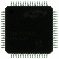
C8051F021-GQ Silicon Laboratories Inc, C8051F021-GQ Datasheet - Page 108

C8051F021-GQ
Manufacturer Part Number
C8051F021-GQ
Description
IC 8051 MCU 64K FLASH 64TQFP
Manufacturer
Silicon Laboratories Inc
Series
C8051F02xr
Specifications of C8051F021-GQ
Program Memory Type
FLASH
Program Memory Size
64KB (64K x 8)
Package / Case
64-TQFP, 64-VQFP
Core Processor
8051
Core Size
8-Bit
Speed
25MHz
Connectivity
EBI/EMI, SMBus (2-Wire/I²C), SPI, UART/USART
Peripherals
Brown-out Detect/Reset, POR, PWM, Temp Sensor, WDT
Number Of I /o
32
Ram Size
4.25K x 8
Voltage - Supply (vcc/vdd)
2.7 V ~ 3.6 V
Data Converters
A/D 8x8b, 8x12b; D/A 2x12b
Oscillator Type
Internal
Operating Temperature
-40°C ~ 85°C
Processor Series
C8051F0x
Core
8051
Data Bus Width
8 bit
Data Ram Size
4.25 KB
Interface Type
I2C/SMBus/SPI/UART
Maximum Clock Frequency
25 MHz
Number Of Programmable I/os
32
Number Of Timers
4
Operating Supply Voltage
2.7 V to 3.6 V
Maximum Operating Temperature
+ 85 C
Mounting Style
SMD/SMT
3rd Party Development Tools
PK51, CA51, A51, ULINK2
Development Tools By Supplier
C8051F020DK
Minimum Operating Temperature
- 40 C
On-chip Adc
8-ch x 8-bit or 8-ch x 12-bit
On-chip Dac
2-ch x 12-bit
No. Of I/o's
32
Ram Memory Size
4352Byte
Cpu Speed
25MHz
No. Of Timers
5
No. Of Pwm Channels
5
Rohs Compliant
Yes
Data Rom Size
64 KB
A/d Bit Size
12 bit
A/d Channels Available
8
Height
1.05 mm
Length
10 mm
Supply Voltage (max)
3.6 V
Supply Voltage (min)
2.7 V
Width
10 mm
Lead Free Status / RoHS Status
Lead free / RoHS Compliant
For Use With
336-1200 - DEV KIT FOR F020/F021/F022/F023
Eeprom Size
-
Lead Free Status / Rohs Status
Lead free / RoHS Compliant
Other names
336-1201
Available stocks
Company
Part Number
Manufacturer
Quantity
Price
Company:
Part Number:
C8051F021-GQ
Manufacturer:
Silicon Laboratories Inc
Quantity:
10 000
Company:
Part Number:
C8051F021-GQR
Manufacturer:
SiliconL
Quantity:
2 000
Company:
Part Number:
C8051F021-GQR
Manufacturer:
Silicon Laboratories Inc
Quantity:
10 000
Part Number:
C8051F021-GQR
Manufacturer:
SILICON LABS/芯科
Quantity:
20 000
C8051F020/1/2/3
12.2.2. Data Memory
The CIP-51 implements 256 bytes of internal RAM mapped into the data memory space from 0x00 through 0xFF.
The lower 128 bytes of data memory are used for general purpose registers and scratch pad memory. Either direct or
indirect addressing may be used to access the lower 128 bytes of data memory. Locations 0x00 through 0x1F are
addressable as four banks of general purpose registers, each bank consisting of eight byte-wide registers. The next
16 bytes, locations 0x20 through 0x2F, may either be addressed as bytes or as 128 bit locations accessible with the
direct addressing mode.
The upper 128 bytes of data memory are accessible only by indirect addressing. This region occupies the same
address space as the Special Function Registers (SFR) but is physically separate from the SFR space. The addressing
mode used by an instruction when accessing locations above 0x7F determines whether the CPU accesses the upper
128 bytes of data memory space or the SFRs. Instructions that use direct addressing will access the SFR space.
Instructions using indirect addressing above 0x7F access the upper 128 bytes of data memory. Figure 12.2 illustrates
the data memory organization of the CIP-51.
12.2.3. General Purpose Registers
The lower 32 bytes of data memory, locations 0x00 through 0x1F, may be addressed as four banks of general-purpose
registers. Each bank consists of eight byte-wide registers designated R0 through R7. Only one of these banks may be
enabled at a time. Two bits in the program status word, RS0 (PSW.3) and RS1 (PSW.4), select the active register bank
(see description of the PSW in Figure 12.6). This allows fast context switching when entering subroutines and inter-
rupt service routines. Indirect addressing modes use registers R0 and R1 as index registers.
12.2.4. Bit Addressable Locations
In addition to direct access to data memory organized as bytes, the sixteen data memory locations at 0x20 through
0x2F are also accessible as 128 individually addressable bits. Each bit has a bit address from 0x00 to 0x7F. Bit 0 of
the byte at 0x20 has bit address 0x00 while bit 7 of the byte at 0x20 has bit address 0x07. Bit 7 of the byte at 0x2F has
bit address 0x7F. A bit access is distinguished from a full byte access by the type of instruction used (bit source or
destination operands as opposed to a byte source or destination).
The MCS-51™ assembly language allows an alternate notation for bit addressing of the form XX.B where XX is the
byte address and B is the bit position within the byte. For example, the instruction:
MOV
C, 22.3h
moves the Boolean value at 0x13 (bit 3 of the byte at location 0x22) into the Carry flag.
12.2.5. Stack
A programmer's stack can be located anywhere in the 256 byte data memory. The stack area is designated using the
Stack Pointer (SP, address 0x81) SFR. The SP will point to the last location used. The next value pushed on the stack
is placed at SP+1 and then SP is incremented. A reset initializes the stack pointer to location 0x07; therefore, the first
value pushed on the stack is placed at location 0x08, which is also the first register (R0) of register bank 1. Thus, if
more than one register bank is to be used, the SP should be initialized to a location in the data memory not being used
for data storage. The stack depth can extend up to 256 bytes.
The MCUs also have built-in hardware for a stack record. The stack record is a 32-bit shift register, where each
PUSH or increment SP pushes one record bit onto the register, and each CALL pushes two record bits onto the regis-
ter. (A POP or decrement SP pops one record bit, and a RET pops two record bits, also.) The stack record circuitry
can also detect an overflow or underflow on the 32-bit shift register, and can notify the debug software even with the
MCU running at speed.
108
Rev. 1.4


