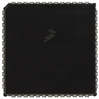
MC68HC711E9CFNE2 Freescale Semiconductor, MC68HC711E9CFNE2 Datasheet - Page 171

MC68HC711E9CFNE2
Manufacturer Part Number
MC68HC711E9CFNE2
Description
IC MCU 8BIT 512RAM 52-PLC
Manufacturer
Freescale Semiconductor
Series
HC11r
Datasheet
1.MC68HC711E9CFNE3.pdf
(336 pages)
Specifications of MC68HC711E9CFNE2
Core Processor
HC11
Core Size
8-Bit
Speed
2MHz
Connectivity
SCI, SPI
Peripherals
POR, WDT
Number Of I /o
38
Program Memory Size
12KB (12K x 8)
Program Memory Type
OTP
Eeprom Size
512 x 8
Ram Size
512 x 8
Voltage - Supply (vcc/vdd)
4.5 V ~ 5.5 V
Data Converters
A/D 8x8b
Oscillator Type
Internal
Operating Temperature
-40°C ~ 85°C
Package / Case
52-PLCC
Processor Series
HC711E
Core
HC11
Data Bus Width
8 bit
Data Ram Size
512 B
Interface Type
SCI, SPI
Maximum Clock Frequency
2 MHz
Number Of Programmable I/os
38
Number Of Timers
8
Maximum Operating Temperature
+ 85 C
Mounting Style
SMD/SMT
Minimum Operating Temperature
- 40 C
On-chip Adc
8 bit
Lead Free Status / RoHS Status
Lead free / RoHS Compliant
Available stocks
Company
Part Number
Manufacturer
Quantity
Price
Company:
Part Number:
MC68HC711E9CFNE2
Manufacturer:
TE
Quantity:
12 000
Company:
Part Number:
MC68HC711E9CFNE2
Manufacturer:
FREESCAL
Quantity:
5 530
- Current page: 171 of 336
- Download datasheet (4Mb)
8.7 SPI System Errors
M68HC11E Family — Rev. 3.2
MOTOROLA
direction register. This sets the SS pin to act as a general-purpose output
rather than the dedicated input to the slave select circuit, thus inhibiting
the mode fault flag. The other three lines are dedicated to the SPI
whenever the serial peripheral interface is on.
The state of the master and slave CPHA bits affects the operation of SS.
CPHA settings should be identical for master and slave. When
CPHA = 0, the shift clock is the OR of SS with SCK. In this clock phase
mode, SS must go high between successive characters in an SPI
message. When CPHA = 1, SS can be left low between successive SPI
characters. In cases where there is only one SPI slave MCU, its SS line
can be tied to V
Two system errors can be detected by the SPI system. The first type of
error arises in a multiple-master system when more than one SPI device
simultaneously tries to be a master. This error is called a mode fault. The
second type of error, write collision, indicates that an attempt was made
to write data to the SPDR while a transfer was in progress.
When the SPI system is configured as a master and the SS input line
goes to active low, a mode fault error has occurred — usually because
two devices have attempted to act as master at the same time. In cases
where more than one device is concurrently configured as a master,
there is a chance of contention between two pin drivers. For push-pull
CMOS drivers, this contention can cause permanent damage. The mode
fault mechanism attempts to protect the device by disabling the drivers.
The MSTR control bit in the SPCR and all four DDRD control bits
associated with the SPI are cleared and an interrupt is generated subject
to masking by the SPIE control bit and the I bit in the CCR.
Other precautions may need to be taken to prevent driver damage. If two
devices are made masters at the same time, mode fault does not help
protect either one unless one of them selects the other as slave. The
amount of damage possible depends on the length of time both devices
attempt to act as master.
Serial Peripheral Interface (SPI)
SS
as long as only CPHA = 1 clock mode is used.
Serial Peripheral Interface (SPI)
SPI System Errors
Technical Data
171
Related parts for MC68HC711E9CFNE2
Image
Part Number
Description
Manufacturer
Datasheet
Request
R

Part Number:
Description:
APPENDIX A ELECTRICAL CHARACTERISTICS
Manufacturer:
FREESCALE [Freescale Semiconductor, Inc]
Datasheet:
Part Number:
Description:
Manufacturer:
Freescale Semiconductor, Inc
Datasheet:
Part Number:
Description:
Manufacturer:
Freescale Semiconductor, Inc
Datasheet:
Part Number:
Description:
Manufacturer:
Freescale Semiconductor, Inc
Datasheet:
Part Number:
Description:
Manufacturer:
Freescale Semiconductor, Inc
Datasheet:
Part Number:
Description:
Manufacturer:
Freescale Semiconductor, Inc
Datasheet:
Part Number:
Description:
Manufacturer:
Freescale Semiconductor, Inc
Datasheet:
Part Number:
Description:
Manufacturer:
Freescale Semiconductor, Inc
Datasheet:
Part Number:
Description:
Manufacturer:
Freescale Semiconductor, Inc
Datasheet:
Part Number:
Description:
Manufacturer:
Freescale Semiconductor, Inc
Datasheet:
Part Number:
Description:
Manufacturer:
Freescale Semiconductor, Inc
Datasheet:
Part Number:
Description:
Manufacturer:
Freescale Semiconductor, Inc
Datasheet:
Part Number:
Description:
Manufacturer:
Freescale Semiconductor, Inc
Datasheet:
Part Number:
Description:
Manufacturer:
Freescale Semiconductor, Inc
Datasheet:
Part Number:
Description:
Manufacturer:
Freescale Semiconductor, Inc
Datasheet:


