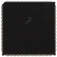
MC68HC711E9CFNE2 Freescale Semiconductor, MC68HC711E9CFNE2 Datasheet - Page 172

MC68HC711E9CFNE2
Manufacturer Part Number
MC68HC711E9CFNE2
Description
IC MCU 8BIT 512RAM 52-PLC
Manufacturer
Freescale Semiconductor
Series
HC11r
Datasheet
1.MC68HC711E9CFNE3.pdf
(336 pages)
Specifications of MC68HC711E9CFNE2
Core Processor
HC11
Core Size
8-Bit
Speed
2MHz
Connectivity
SCI, SPI
Peripherals
POR, WDT
Number Of I /o
38
Program Memory Size
12KB (12K x 8)
Program Memory Type
OTP
Eeprom Size
512 x 8
Ram Size
512 x 8
Voltage - Supply (vcc/vdd)
4.5 V ~ 5.5 V
Data Converters
A/D 8x8b
Oscillator Type
Internal
Operating Temperature
-40°C ~ 85°C
Package / Case
52-PLCC
Processor Series
HC711E
Core
HC11
Data Bus Width
8 bit
Data Ram Size
512 B
Interface Type
SCI, SPI
Maximum Clock Frequency
2 MHz
Number Of Programmable I/os
38
Number Of Timers
8
Maximum Operating Temperature
+ 85 C
Mounting Style
SMD/SMT
Minimum Operating Temperature
- 40 C
On-chip Adc
8 bit
Lead Free Status / RoHS Status
Lead free / RoHS Compliant
Available stocks
Company
Part Number
Manufacturer
Quantity
Price
Company:
Part Number:
MC68HC711E9CFNE2
Manufacturer:
TE
Quantity:
12 000
Company:
Part Number:
MC68HC711E9CFNE2
Manufacturer:
FREESCAL
Quantity:
5 530
- Current page: 172 of 336
- Download datasheet (4Mb)
Serial Peripheral Interface (SPI)
8.8 SPI Registers
Technical Data
172
A write collision error occurs if the SPDR is written while a transfer is in
progress. Because the SPDR is not double buffered in the transmit
direction, writes to SPDR cause data to be written directly into the SPI
shift register. Because this write corrupts any transfer in progress, a
write collision error is generated. The transfer continues undisturbed,
and the write data that caused the error is not written to the shifter.
A write collision is normally a slave error because a slave has no control
over when a master initiates a transfer. A master knows when a transfer
is in progress, so there is no reason for a master to generate a
write-collision error, although the SPI logic can detect write collisions in
both master and slave devices.
The SPI configuration determines the characteristics of a transfer in
progress. For a master, a transfer begins when data is written to SPDR
and ends when SPIF is set. For a slave with CPHA equal to 0, a transfer
starts when SS goes low and ends when SS returns high. In this case,
SPIF is set at the middle of the eighth SCK cycle when data is
transferred from the shifter to the parallel data register, but the transfer
is still in progress until SS goes high. For a slave with CPHA equal to 1,
transfer begins when the SCK line goes to its active level, which is the
edge at the beginning of the first SCK cycle. The transfer ends in a slave
in which CPHA equals 1 when SPIF is set.
The three SPI registers are:
These registers provide control, status, and data storage functions.
•
•
•
Serial peripheral control register (SPCR)
Serial peripheral status register (SPSR)
Serial peripheral data register (SPDR)
Serial Peripheral Interface (SPI)
M68HC11E Family — Rev. 3.2
MOTOROLA
Related parts for MC68HC711E9CFNE2
Image
Part Number
Description
Manufacturer
Datasheet
Request
R

Part Number:
Description:
APPENDIX A ELECTRICAL CHARACTERISTICS
Manufacturer:
FREESCALE [Freescale Semiconductor, Inc]
Datasheet:
Part Number:
Description:
Manufacturer:
Freescale Semiconductor, Inc
Datasheet:
Part Number:
Description:
Manufacturer:
Freescale Semiconductor, Inc
Datasheet:
Part Number:
Description:
Manufacturer:
Freescale Semiconductor, Inc
Datasheet:
Part Number:
Description:
Manufacturer:
Freescale Semiconductor, Inc
Datasheet:
Part Number:
Description:
Manufacturer:
Freescale Semiconductor, Inc
Datasheet:
Part Number:
Description:
Manufacturer:
Freescale Semiconductor, Inc
Datasheet:
Part Number:
Description:
Manufacturer:
Freescale Semiconductor, Inc
Datasheet:
Part Number:
Description:
Manufacturer:
Freescale Semiconductor, Inc
Datasheet:
Part Number:
Description:
Manufacturer:
Freescale Semiconductor, Inc
Datasheet:
Part Number:
Description:
Manufacturer:
Freescale Semiconductor, Inc
Datasheet:
Part Number:
Description:
Manufacturer:
Freescale Semiconductor, Inc
Datasheet:
Part Number:
Description:
Manufacturer:
Freescale Semiconductor, Inc
Datasheet:
Part Number:
Description:
Manufacturer:
Freescale Semiconductor, Inc
Datasheet:
Part Number:
Description:
Manufacturer:
Freescale Semiconductor, Inc
Datasheet:


