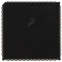
MC68HC711E9CFNE2 Freescale Semiconductor, MC68HC711E9CFNE2 Datasheet - Page 34

MC68HC711E9CFNE2
Manufacturer Part Number
MC68HC711E9CFNE2
Description
IC MCU 8BIT 512RAM 52-PLC
Manufacturer
Freescale Semiconductor
Series
HC11r
Datasheet
1.MC68HC711E9CFNE3.pdf
(336 pages)
Specifications of MC68HC711E9CFNE2
Core Processor
HC11
Core Size
8-Bit
Speed
2MHz
Connectivity
SCI, SPI
Peripherals
POR, WDT
Number Of I /o
38
Program Memory Size
12KB (12K x 8)
Program Memory Type
OTP
Eeprom Size
512 x 8
Ram Size
512 x 8
Voltage - Supply (vcc/vdd)
4.5 V ~ 5.5 V
Data Converters
A/D 8x8b
Oscillator Type
Internal
Operating Temperature
-40°C ~ 85°C
Package / Case
52-PLCC
Processor Series
HC711E
Core
HC11
Data Bus Width
8 bit
Data Ram Size
512 B
Interface Type
SCI, SPI
Maximum Clock Frequency
2 MHz
Number Of Programmable I/os
38
Number Of Timers
8
Maximum Operating Temperature
+ 85 C
Mounting Style
SMD/SMT
Minimum Operating Temperature
- 40 C
On-chip Adc
8 bit
Lead Free Status / RoHS Status
Lead free / RoHS Compliant
Available stocks
Company
Part Number
Manufacturer
Quantity
Price
Company:
Part Number:
MC68HC711E9CFNE2
Manufacturer:
TE
Quantity:
12 000
Company:
Part Number:
MC68HC711E9CFNE2
Manufacturer:
FREESCAL
Quantity:
5 530
- Current page: 34 of 336
- Download datasheet (4Mb)
Pin Descriptions
2.4 RESET
Technical Data
34
CAUTION:
A bidirectional control signal, RESET, acts as an input to initialize the
MCU to a known startup state. It also acts as an open-drain output to
indicate that an internal failure has been detected in either the clock
monitor or computer operating properly (COP) watchdog circuit. The
CPU distinguishes between internal and external reset conditions by
sensing whether the reset pin rises to a logic 1 in less than two E-clock
cycles after a reset has occurred. See
Do not connect an external resistor capacitor (RC) power-up delay
circuit to the reset pin of M68HC11 devices because the circuit charge
time constant can cause the device to misinterpret the type of reset that
occurred.
Because the CPU is not able to fetch and execute instructions properly
when V
be controlled. A low-voltage inhibit (LVI) circuit is required primarily for
protection of EEPROM contents. However, since the configuration
register (CONFIG) value is read from the EEPROM, protection is
required even if the EEPROM array is not being used.
Presently, there are several economical ways to solve this problem. For
example, two good external components for LVI reset are:
Refer to
1. The Seiko S0854HN (or other S805 series devices):
2. The Motorola MC34064:
— Extremely low power (2 A)
— TO-92 package
— Limited temperature range, –20 C to +70 C
— Available in various trip-point voltage ranges
— TO-92 or SO-8 package
— Draws about 300 A
— Temperature range –40 C to 85 C
— Well controlled trip point
— Inexpensive
DD
Section 5. Resets and Interrupts
falls below the minimum operating voltage level, reset must
Pin Descriptions
Figure 2-6
for further information.
M68HC11E Family — Rev. 3.2
and
Figure
MOTOROLA
2-7.
Related parts for MC68HC711E9CFNE2
Image
Part Number
Description
Manufacturer
Datasheet
Request
R

Part Number:
Description:
APPENDIX A ELECTRICAL CHARACTERISTICS
Manufacturer:
FREESCALE [Freescale Semiconductor, Inc]
Datasheet:
Part Number:
Description:
Manufacturer:
Freescale Semiconductor, Inc
Datasheet:
Part Number:
Description:
Manufacturer:
Freescale Semiconductor, Inc
Datasheet:
Part Number:
Description:
Manufacturer:
Freescale Semiconductor, Inc
Datasheet:
Part Number:
Description:
Manufacturer:
Freescale Semiconductor, Inc
Datasheet:
Part Number:
Description:
Manufacturer:
Freescale Semiconductor, Inc
Datasheet:
Part Number:
Description:
Manufacturer:
Freescale Semiconductor, Inc
Datasheet:
Part Number:
Description:
Manufacturer:
Freescale Semiconductor, Inc
Datasheet:
Part Number:
Description:
Manufacturer:
Freescale Semiconductor, Inc
Datasheet:
Part Number:
Description:
Manufacturer:
Freescale Semiconductor, Inc
Datasheet:
Part Number:
Description:
Manufacturer:
Freescale Semiconductor, Inc
Datasheet:
Part Number:
Description:
Manufacturer:
Freescale Semiconductor, Inc
Datasheet:
Part Number:
Description:
Manufacturer:
Freescale Semiconductor, Inc
Datasheet:
Part Number:
Description:
Manufacturer:
Freescale Semiconductor, Inc
Datasheet:
Part Number:
Description:
Manufacturer:
Freescale Semiconductor, Inc
Datasheet:


