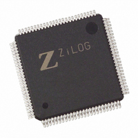
EZ80190AZ050SC00TR Zilog, EZ80190AZ050SC00TR Datasheet - Page 135

EZ80190AZ050SC00TR
Manufacturer Part Number
EZ80190AZ050SC00TR
Description
IC EZ80 ACCLAIM 50MHZ 100LQFP
Manufacturer
Zilog
Datasheet
1.EZ80190AZ050SG.pdf
(221 pages)
Specifications of EZ80190AZ050SC00TR
Processor Type
eZ80
Features
High Speed, Single-Cycle Instruction-Fetch
Speed
50MHz
Voltage
3.3V
Mounting Type
Surface Mount
Package / Case
100-LQFP
Lead Free Status / RoHS Status
Contains lead / RoHS non-compliant
Available stocks
Company
Part Number
Manufacturer
Quantity
Price
- Current page: 135 of 221
- Download datasheet (4Mb)
MACC RAM
MACC RAM Address Indexing
PS006614-1208
2. If the DATA bank status is EMPTY and the CALC bank status is DONE, write
3. If both status fields indicate EMPTY, there is no result to retrieve.
4. If the DATA bank status is DONE, the application reads as many of the MAC_AC0–3
The eZ80190 device features 1 KB of dual-port RAM available for use with the Multiply-
Accumulator, as displayed in
appears as a 1 KB block of 8-bit RAM. To the Multiply-Accumulator, MACC RAM
appears as two blocks of 256 x 16-bit RAM. The CPU provides Read/Write access to one
port of the MACC RAM. The Multiply-Accumulator provides Read Only access to the
second port of the MACC RAM.
As described in
CPU in the memory address space from {RAM_ADDR_U[7:0],
{RAM_ADDR_U[7:0],
from the RAM Address Upper Byte register, RAM_ADDR_U. The MACC X data is
stored in the lower 512 bytes of the MACC RAM memory address space from
DDFFh
address space from
stored in the even memory addresses. The MSB, bits [15:8], are stored in the odd memory
addresses. The data in MACC RAM must be stored in two’s-complement form.
For each calculation that the MACC is to perform, the software must arrange the two vec-
tors/arrays to be multiplied and accumulated. One vector must be written to x RAM while
the other vector must be written to y RAM. The software then writes values to the MACC
control registers to indicate where the x and y data is to be stored for the current calcula-
tion. For both x and y data, there are 3 values defining the data location:
1. MACC_xSTART and MACC_ySTART define the address of the first x and y values to
the status register. As a result, the register banks are swapped so that the DATA status
becomes DONE.
registers as desired. Because the Multiply-Accumulator decodes the A15:8 lines to
determine when a transfer is complete, this register READ can be initiated with an
INI2R instruction. Reading the final byte of the result changes the DATA bank status
to EMPTY unless there is another result to retrieve. If such is the case, the CALC
bank status changes to EMPTY and the DATA bank status changes to DONE.
be multiplied together.
. The MACC y data is stored in the upper 512 bytes of the MACC RAM memory
Random Access Memory
DE00h
DFFFh
to
Figure 23
DFFFh
}. The upper byte of the MACC RAM address is received
. The LSB, bits [7:0] of the 16-bit x and y data, is
on page 126. From the CPU, MACC RAM
on page 59 , MACC RAM is accessed by the
Product Specification
DC00h
Multiply-Accumulator
} to
DC00h
eZ80190
80h
to
to
125
Related parts for EZ80190AZ050SC00TR
Image
Part Number
Description
Manufacturer
Datasheet
Request
R

Part Number:
Description:
Communication Controllers, ZILOG INTELLIGENT PERIPHERAL CONTROLLER (ZIP)
Manufacturer:
Zilog, Inc.
Datasheet:

Part Number:
Description:
KIT DEV FOR Z8 ENCORE 16K TO 64K
Manufacturer:
Zilog
Datasheet:

Part Number:
Description:
KIT DEV Z8 ENCORE XP 28-PIN
Manufacturer:
Zilog
Datasheet:

Part Number:
Description:
DEV KIT FOR Z8 ENCORE 8K/4K
Manufacturer:
Zilog
Datasheet:

Part Number:
Description:
KIT DEV Z8 ENCORE XP 28-PIN
Manufacturer:
Zilog
Datasheet:

Part Number:
Description:
DEV KIT FOR Z8 ENCORE 4K TO 8K
Manufacturer:
Zilog
Datasheet:

Part Number:
Description:
CMOS Z8 microcontroller. ROM 16 Kbytes, RAM 256 bytes, speed 16 MHz, 32 lines I/O, 3.0V to 5.5V
Manufacturer:
Zilog, Inc.
Datasheet:

Part Number:
Description:
Low-cost microcontroller. 512 bytes ROM, 61 bytes RAM, 8 MHz
Manufacturer:
Zilog, Inc.
Datasheet:

Part Number:
Description:
Z8 4K OTP Microcontroller
Manufacturer:
Zilog, Inc.
Datasheet:

Part Number:
Description:
CMOS SUPER8 ROMLESS MCU
Manufacturer:
Zilog, Inc.
Datasheet:

Part Number:
Description:
SL1866 CMOSZ8 OTP Microcontroller
Manufacturer:
Zilog, Inc.
Datasheet:

Part Number:
Description:
SL1866 CMOSZ8 OTP Microcontroller
Manufacturer:
Zilog, Inc.
Datasheet:

Part Number:
Description:
OTP (KB) = 1, RAM = 125, Speed = 12, I/O = 14, 8-bit Timers = 2, Comm Interfaces Other Features = Por, LV Protect, Voltage = 4.5-5.5V
Manufacturer:
Zilog, Inc.
Datasheet:

Part Number:
Description:
Manufacturer:
Zilog, Inc.
Datasheet:


