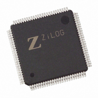
EZ80190AZ050SC00TR Zilog, EZ80190AZ050SC00TR Datasheet - Page 95

EZ80190AZ050SC00TR
Manufacturer Part Number
EZ80190AZ050SC00TR
Description
IC EZ80 ACCLAIM 50MHZ 100LQFP
Manufacturer
Zilog
Datasheet
1.EZ80190AZ050SG.pdf
(221 pages)
Specifications of EZ80190AZ050SC00TR
Processor Type
eZ80
Features
High Speed, Single-Cycle Instruction-Fetch
Speed
50MHz
Voltage
3.3V
Mounting Type
Surface Mount
Package / Case
100-LQFP
Lead Free Status / RoHS Status
Contains lead / RoHS non-compliant
Available stocks
Company
Part Number
Manufacturer
Quantity
Price
- Current page: 95 of 221
- Download datasheet (4Mb)
PS006614-1208
Master Out Slave In
Slave Select
Serial Clock
is not selected. When the SPI is not enabled by the UZI Control register, this signal oper-
ates in a high-impedance state.
The Master Out Slave In (MOSI) pin is configured as an output in a master device and as
an input in a slave device. It is one of the two lines that transfer serial data, with the msb
sent first. When the SPI is not enabled by the UZI Control register, this signal operates in a
high-impedance state.
The active Low Slave Select (SS) input signal is used to select a slave SPI device. It must
be operating in a Low state prior to all data communication and must stay Low for the
duration of the data transfer.
The SS input signal on the master must be in a High state. If the SS signal goes Low, a
Mode Fault error flag (MODF bit) is set in the SPIx_SR register. For more information see
SPI Status Register
When the SPI Clock Phase (CPHA) bit = 0, the shift clock is the OR of SS with SCK. In
this clock phase mode, SS must go High between successive characters in an SPI message.
When CPHA = 1, SS can remain Low for several SPI characters. In cases where there is
only one SPI slave MCU, its SS line could be tied Low as long as CPHA = 1 CLOCK
mode is used. For more information on the CPHA bit see
=
The Serial Clock (SCK) is used to synchronize data movement both in and out of the
device through its MOSI and MISO pins. The master and slave are each capable of
exchanging a byte of data during a sequence of eight clock cycles. Because SCK is gener-
ated by the master, the SCK pin becomes an input on a slave device. The SPI contains an
internal divide-by-two clock divider. The SPI serial clock is one-half the frequency of the
clock signal created by the UZI Baud Rate Generator, as shown by the following equation:
As displayed in
tions may be selected when using control bits CPOL and CPHA in the SPI Control regis-
ter. See
B6h
SPI Data Transfer Rate (bits/s) =
, SPI1_CTL =
SPI Control Register
Figure 14
(SPI0_SR =
BAh
) on page 89 .
on page 86 and
(SPI0_CTL =
B7h
, SPI1_SR =
2 x Baud Rate Generator Divisor
System Clock Frequency
Table 38
B6h
, SPI1_CTL =
BBh
on page 86, four possible timing rela-
) on page 90 .
SPI Control Register
BAh
Product Specification
Serial Peripheral Interface
) on page 89. Both the
(SPI0_CTL
eZ80190
85
Related parts for EZ80190AZ050SC00TR
Image
Part Number
Description
Manufacturer
Datasheet
Request
R

Part Number:
Description:
Communication Controllers, ZILOG INTELLIGENT PERIPHERAL CONTROLLER (ZIP)
Manufacturer:
Zilog, Inc.
Datasheet:

Part Number:
Description:
KIT DEV FOR Z8 ENCORE 16K TO 64K
Manufacturer:
Zilog
Datasheet:

Part Number:
Description:
KIT DEV Z8 ENCORE XP 28-PIN
Manufacturer:
Zilog
Datasheet:

Part Number:
Description:
DEV KIT FOR Z8 ENCORE 8K/4K
Manufacturer:
Zilog
Datasheet:

Part Number:
Description:
KIT DEV Z8 ENCORE XP 28-PIN
Manufacturer:
Zilog
Datasheet:

Part Number:
Description:
DEV KIT FOR Z8 ENCORE 4K TO 8K
Manufacturer:
Zilog
Datasheet:

Part Number:
Description:
CMOS Z8 microcontroller. ROM 16 Kbytes, RAM 256 bytes, speed 16 MHz, 32 lines I/O, 3.0V to 5.5V
Manufacturer:
Zilog, Inc.
Datasheet:

Part Number:
Description:
Low-cost microcontroller. 512 bytes ROM, 61 bytes RAM, 8 MHz
Manufacturer:
Zilog, Inc.
Datasheet:

Part Number:
Description:
Z8 4K OTP Microcontroller
Manufacturer:
Zilog, Inc.
Datasheet:

Part Number:
Description:
CMOS SUPER8 ROMLESS MCU
Manufacturer:
Zilog, Inc.
Datasheet:

Part Number:
Description:
SL1866 CMOSZ8 OTP Microcontroller
Manufacturer:
Zilog, Inc.
Datasheet:

Part Number:
Description:
SL1866 CMOSZ8 OTP Microcontroller
Manufacturer:
Zilog, Inc.
Datasheet:

Part Number:
Description:
OTP (KB) = 1, RAM = 125, Speed = 12, I/O = 14, 8-bit Timers = 2, Comm Interfaces Other Features = Por, LV Protect, Voltage = 4.5-5.5V
Manufacturer:
Zilog, Inc.
Datasheet:

Part Number:
Description:
Manufacturer:
Zilog, Inc.
Datasheet:


