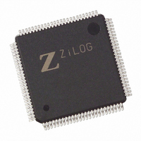
EZ80190AZ050SC00TR Zilog, EZ80190AZ050SC00TR Datasheet - Page 16

EZ80190AZ050SC00TR
Manufacturer Part Number
EZ80190AZ050SC00TR
Description
IC EZ80 ACCLAIM 50MHZ 100LQFP
Manufacturer
Zilog
Datasheet
1.EZ80190AZ050SG.pdf
(221 pages)
Specifications of EZ80190AZ050SC00TR
Processor Type
eZ80
Features
High Speed, Single-Cycle Instruction-Fetch
Speed
50MHz
Voltage
3.3V
Mounting Type
Surface Mount
Package / Case
100-LQFP
Lead Free Status / RoHS Status
Contains lead / RoHS non-compliant
Available stocks
Company
Part Number
Manufacturer
Quantity
Price
- Current page: 16 of 221
- Download datasheet (4Mb)
Table 1. 100-Pin LQFP Pin Identification of the eZ80190 Device (Continued)
PS006614-1208
Pin
No.
10
11
12
13
14
15
Symbol
ADDR0
ADDR1
ADDR2
ADDR3
ADDR4
ADDR5
Function
Address Bus
Address Bus
Address Bus
Address Bus
Address Bus
Address Bus
Signal Direction
Input/Output
Input/Output
Input/Output
Input/Output
Input/Output
Input/Output
Description
The ADDR0 is configured as an output in normal
operation. The address bus selects a location in
memory or I/O space to be read or written. This
pin is configured as an input during bus
acknowledge cycles. Drives the Chip Select/Wait
State Generator block to generate Chip Selects.
The ADDR1 pin is configured as an output in
normal operation. The address bus selects a
location in memory or I/O space to be read or
written. This pin is configured as an input during
bus acknowledge cycles. Drives the Chip Select/
Wait State Generator block to generate Chip
Selects.
The ADDR2 pin is configured as an output in
normal operation. The address bus selects a
location in memory or I/O space to be read or
written. This pin is configured as an input during
bus acknowledge cycles. Drives the Chip Select/
Wait State Generator block to generate Chip
Selects.
The ADDR3 pin is configured as an output in
normal operation. The address bus selects a
location in memory or I/O space to be read or
written. This pin is configured as an input during
bus acknowledge cycles. Drives the Chip Select/
Wait State Generator block to generate Chip
Selects.
The ADDR4 pin is configured as an output in
normal operation. The address bus selects a
location in memory or I/O space to be read or
written. This pin is configured as an input during
bus acknowledge cycles. Drives the Chip Select/
Wait State Generator block to generate Chip
Selects.
The ADDR5 pin is configured as an output in
normal operation. The address bus selects a
location in memory or I/O space to be read or
written. This pin is configured as an input during
bus acknowledge cycles. Drives the Chip Select/
Wait State Generator block to generate Chip
Selects.
Product Specification
Architectural Overview
6
Related parts for EZ80190AZ050SC00TR
Image
Part Number
Description
Manufacturer
Datasheet
Request
R

Part Number:
Description:
Communication Controllers, ZILOG INTELLIGENT PERIPHERAL CONTROLLER (ZIP)
Manufacturer:
Zilog, Inc.
Datasheet:

Part Number:
Description:
KIT DEV FOR Z8 ENCORE 16K TO 64K
Manufacturer:
Zilog
Datasheet:

Part Number:
Description:
KIT DEV Z8 ENCORE XP 28-PIN
Manufacturer:
Zilog
Datasheet:

Part Number:
Description:
DEV KIT FOR Z8 ENCORE 8K/4K
Manufacturer:
Zilog
Datasheet:

Part Number:
Description:
KIT DEV Z8 ENCORE XP 28-PIN
Manufacturer:
Zilog
Datasheet:

Part Number:
Description:
DEV KIT FOR Z8 ENCORE 4K TO 8K
Manufacturer:
Zilog
Datasheet:

Part Number:
Description:
CMOS Z8 microcontroller. ROM 16 Kbytes, RAM 256 bytes, speed 16 MHz, 32 lines I/O, 3.0V to 5.5V
Manufacturer:
Zilog, Inc.
Datasheet:

Part Number:
Description:
Low-cost microcontroller. 512 bytes ROM, 61 bytes RAM, 8 MHz
Manufacturer:
Zilog, Inc.
Datasheet:

Part Number:
Description:
Z8 4K OTP Microcontroller
Manufacturer:
Zilog, Inc.
Datasheet:

Part Number:
Description:
CMOS SUPER8 ROMLESS MCU
Manufacturer:
Zilog, Inc.
Datasheet:

Part Number:
Description:
SL1866 CMOSZ8 OTP Microcontroller
Manufacturer:
Zilog, Inc.
Datasheet:

Part Number:
Description:
SL1866 CMOSZ8 OTP Microcontroller
Manufacturer:
Zilog, Inc.
Datasheet:

Part Number:
Description:
OTP (KB) = 1, RAM = 125, Speed = 12, I/O = 14, 8-bit Timers = 2, Comm Interfaces Other Features = Por, LV Protect, Voltage = 4.5-5.5V
Manufacturer:
Zilog, Inc.
Datasheet:

Part Number:
Description:
Manufacturer:
Zilog, Inc.
Datasheet:


