MPC8572DS Freescale Semiconductor, MPC8572DS Datasheet - Page 119
MPC8572DS
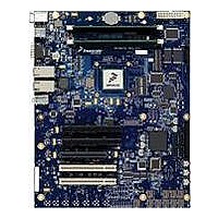
Manufacturer Part Number
MPC8572DS
Description
KIT MPU POWERQUICC III
Manufacturer
Freescale Semiconductor
Series
PowerQUICC III™r
Type
MPUr
Specifications of MPC8572DS
Contents
Board
Data Rate
10 Mbps to 100 Mbps
Memory Type
Flash, DDR, DDR2, DDR3, SDRAM
Interface Type
I2C, Ethernet
Operating Voltage
3.3 V
Data Bus Width
32 bit
Product
Development Tools
Silicon Manufacturer
Freescale
Core Architecture
Power Architecture
Core Sub-architecture
PowerQUICC
Silicon Core Number
MPC85xx
Silicon Family Name
PowerQUICC III
Rohs Compliant
Yes
For Use With/related Products
MPC8572E
Lead Free Status / RoHS Status
Lead free / RoHS Compliant


Table 80
is determined by the binary value of LBCTL, LALE and LGPL2/LOE/LFRE at power up, as shown in
Table
Table 81
is determined by the binary value of LWE[0]/LBS[0]/LFWE, UART_SOUT[1], and READY_P1 signals
at power up, as shown in
19.4
The dual DDR memory controller complexes can be synchronous with, or asynchronous to, the CCB,
depending on configuration.
Table 82
reference clock, DDRCLK, which is not the memory bus clock. The DDR memory controller complexes
clock frequency is equal to the DDR data rate.
When synchronous mode is selected, the memory buses are clocked at half the CCB clock rate. The default
mode of operation is for the DDR data rate for both DDR controllers to be equal to the CCB clock rate in
synchronous mode, or the resulting DDR PLL rate in asynchronous mode.
In asynchronous mode, the DDR PLL rate to DDRCLK ratios listed in
to DDRCLK ratio, because the DDR PLL rate in asynchronous mode means the DDR data rate resulting
from DDR PLL output.
Freescale Semiconductor
LFWE, UART_SOUT[1],
READY_P1 Signals
Binary Value of
LWE[0]/LBS[0]/
80.
LGPL2/LOE/LFRE
Binary Value of
LBCTL, LALE,
describes the clock ratio between e500 Core0 and the e500 core complex bus (CCB). This ratio
describes the clock ratio between e500 Core1 and the e500 core complex bus (CCB). This ratio
describes the clock ratio between the DDR memory controller complexes and the DDR PLL
DDR/DDRCLK PLL Ratio
000
001
010
011
Signals
000
001
010
011
MPC8572E PowerQUICC III Integrated Processor Hardware Specifications, Rev. 5
Table
e500 Core1:CCB Clock Ratio
e500 Core0:CCB Clock Ratio
81.
Table 80. e500 Core0 to CCB Clock Ratio
Table 81. e500 Core1 to CCB Clock Ratio
3:2 (1.5:1)
Reserved
Reserved
Reserved
3:2 (1.5:1)
Reserved
Reserved
Reserved
LGPL2/LOE/LFRE
LFWE, UART_SOUT[1],
Binary Value of
LBCTL, LALE,
READY_P1 Signals
Binary Value of
LWE[0]/LBS[0]/
Signals
100
101
110
111
100
101
110
111
Table 82
e500 Core0:CCB Clock Ratio
e500 Core1:CCB Clock Ratio
reflects the DDR data rate
5:2 (2.5:1)
7:2 (3.5:1)
2:1
3:1
5:2 (2.5:1)
7:2 (3.5:1)
2:1
3:1
Clocking
119
Related parts for MPC8572DS
Image
Part Number
Description
Manufacturer
Datasheet
Request
R

Part Number:
Description:
Manufacturer:
Freescale Semiconductor, Inc
Datasheet:
Part Number:
Description:
Manufacturer:
Freescale Semiconductor, Inc
Datasheet:
Part Number:
Description:
Manufacturer:
Freescale Semiconductor, Inc
Datasheet:
Part Number:
Description:
Manufacturer:
Freescale Semiconductor, Inc
Datasheet:
Part Number:
Description:
Manufacturer:
Freescale Semiconductor, Inc
Datasheet:
Part Number:
Description:
Manufacturer:
Freescale Semiconductor, Inc
Datasheet:
Part Number:
Description:
Manufacturer:
Freescale Semiconductor, Inc
Datasheet:
Part Number:
Description:
Manufacturer:
Freescale Semiconductor, Inc
Datasheet:
Part Number:
Description:
Manufacturer:
Freescale Semiconductor, Inc
Datasheet:
Part Number:
Description:
Manufacturer:
Freescale Semiconductor, Inc
Datasheet:
Part Number:
Description:
Manufacturer:
Freescale Semiconductor, Inc
Datasheet:
Part Number:
Description:
Manufacturer:
Freescale Semiconductor, Inc
Datasheet:
Part Number:
Description:
Manufacturer:
Freescale Semiconductor, Inc
Datasheet:
Part Number:
Description:
Manufacturer:
Freescale Semiconductor, Inc
Datasheet:
Part Number:
Description:
Manufacturer:
Freescale Semiconductor, Inc
Datasheet: