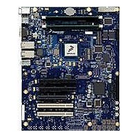
MPC8572DS Freescale Semiconductor, MPC8572DS Datasheet - Page 13

MPC8572DS
Manufacturer Part Number
MPC8572DS
Description
KIT MPU POWERQUICC III
Manufacturer
Freescale Semiconductor
Series
PowerQUICC III™r
Type
MPUr
Specifications of MPC8572DS
Contents
Board
Data Rate
10 Mbps to 100 Mbps
Memory Type
Flash, DDR, DDR2, DDR3, SDRAM
Interface Type
I2C, Ethernet
Operating Voltage
3.3 V
Data Bus Width
32 bit
Product
Development Tools
Silicon Manufacturer
Freescale
Core Architecture
Power Architecture
Core Sub-architecture
PowerQUICC
Silicon Core Number
MPC85xx
Silicon Family Name
PowerQUICC III
Rohs Compliant
Yes
For Use With/related Products
MPC8572E
Lead Free Status / RoHS Status
Lead free / RoHS Compliant
- Current page: 13 of 138
- Download datasheet (2Mb)
Figure 2
The core voltage must always be provided at nominal 1.1 V. (See
voltage.) Voltage to the processor interface I/Os are provided through separate sets of supply pins and must
be provided at the voltages shown in
associated I/O supply voltage. TV
circuits and satisfy appropriate LVCMOS type specifications. The DDR2 and DDR3 SDRAM interface
uses differential receivers referenced by the externally supplied MV
as is appropriate for the SSTL_1.8 electrical signaling standard for DDR2 or 1.5-V electrical signaling for
DDR3. The DDR DQS receivers cannot be operated in single-ended fashion. The complement signal must
be properly driven and cannot be grounded.
Freescale Semiconductor
shows the undershoot and overshoot voltages at the interfaces of the MPC8572E.
VIH
Figure 2. Overshoot/Undershoot Voltage for TV
MPC8572E PowerQUICC III Integrated Processor Hardware Specifications, Rev. 5
VIL
Note:
t
For I
For DDR, t
For eTSEC, t
For eLBC, t
T/B/G/L/OV
CLOCK
T/B/G/L/OV
2
C and JTAG, t
T/B/G/L/OV
refers to the clock period associated with the respective interface:
GND – 0.3 V
GND – 0.7 V
CLOCK
CLOCK
DD
DD
CLOCK
DD
+ 20%
+ 5%
GND
references MCLK.
, BV
references LCLK.
Table
DD
CLOCK
references EC_GTX_CLK125.
DD
2. The input voltage threshold scales with respect to the
references SYSCLK.
, OV
DD
, and LV
Not to Exceed 10%
of t
DD
CLOCK
DD
based receivers are simple CMOS I/O
/BV
Table 2
REF
1
DD
n signal (nominally set to GV
/GV
for actual recommended core
DD
/LV
DD
/OV
Electrical Characteristics
DD
DD
/2)
13
Related parts for MPC8572DS
Image
Part Number
Description
Manufacturer
Datasheet
Request
R
Part Number:
Description:
Manufacturer:
Freescale Semiconductor, Inc
Datasheet:
Part Number:
Description:
Manufacturer:
Freescale Semiconductor, Inc
Datasheet:
Part Number:
Description:
Manufacturer:
Freescale Semiconductor, Inc
Datasheet:
Part Number:
Description:
Manufacturer:
Freescale Semiconductor, Inc
Datasheet:
Part Number:
Description:
Manufacturer:
Freescale Semiconductor, Inc
Datasheet:
Part Number:
Description:
Manufacturer:
Freescale Semiconductor, Inc
Datasheet:
Part Number:
Description:
Manufacturer:
Freescale Semiconductor, Inc
Datasheet:
Part Number:
Description:
Manufacturer:
Freescale Semiconductor, Inc
Datasheet:
Part Number:
Description:
Manufacturer:
Freescale Semiconductor, Inc
Datasheet:
Part Number:
Description:
Manufacturer:
Freescale Semiconductor, Inc
Datasheet:
Part Number:
Description:
Manufacturer:
Freescale Semiconductor, Inc
Datasheet:
Part Number:
Description:
Manufacturer:
Freescale Semiconductor, Inc
Datasheet:
Part Number:
Description:
Manufacturer:
Freescale Semiconductor, Inc
Datasheet:
Part Number:
Description:
Manufacturer:
Freescale Semiconductor, Inc
Datasheet:
Part Number:
Description:
Manufacturer:
Freescale Semiconductor, Inc
Datasheet:


