MPC8572DS Freescale Semiconductor, MPC8572DS Datasheet - Page 86
MPC8572DS
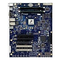
Manufacturer Part Number
MPC8572DS
Description
KIT MPU POWERQUICC III
Manufacturer
Freescale Semiconductor
Series
PowerQUICC III™r
Type
MPUr
Specifications of MPC8572DS
Contents
Board
Data Rate
10 Mbps to 100 Mbps
Memory Type
Flash, DDR, DDR2, DDR3, SDRAM
Interface Type
I2C, Ethernet
Operating Voltage
3.3 V
Data Bus Width
32 bit
Product
Development Tools
Silicon Manufacturer
Freescale
Core Architecture
Power Architecture
Core Sub-architecture
PowerQUICC
Silicon Core Number
MPC85xx
Silicon Family Name
PowerQUICC III
Rohs Compliant
Yes
For Use With/related Products
MPC8572E
Lead Free Status / RoHS Status
Lead free / RoHS Compliant


PCI Express
16.4.3
Table 63
specified at the component pins.
86
UI
V
T
T
-JITTER
V
RL
RL
Z
Z
Z
V
RX-EYE
RX-EYE-MEDIAN-to-MAX
RX-DIFF-DC
RX-DC
RX-HIGH-IMP-DC
RX-DIFFp-p
RX-CM-ACp
RX-IDLE-DET-DIFFp-p
RX-DIFF
RX-CM
Symbol
defines the specifications for the differential input at all receivers (RXs). The parameters are
Differential Receiver (RX) Input Specifications
MPC8572E PowerQUICC III Integrated Processor Hardware Specifications, Rev. 5
Unit Interval
Differential Input
Peak-to-Peak
Voltage
Minimum
Receiver Eye
Width
Maximum time
between the jitter
median and
maximum
deviation from
the median.
AC Peak
Common Mode
Input Voltage
Differential
Return Loss
Common Mode
Return Loss
DC Differential
Input Impedance
DC Input
Impedance
Powered Down
DC Input
Impedance
Electrical Idle
Detect Threshold
Parameter
Table 63. Differential Receiver (RX) Input Specifications
399.88
0.175
200 k
Min
0.4
15
80
40
65
—
—
6
Nominal
400
100
50
—
—
—
—
—
—
—
—
400.12
1.200
Max
150
120
175
0.3
60
—
—
—
—
Units
mV
mV
dB
dB
ps
UI
UI
Ω
Ω
Ω
V
Each UI is 400 ps ± 300 ppm. UI does not
account for Spread Spectrum Clock
dictated variations. See Note 1.
V
See Note 2.
The maximum interconnect media and
Transmitter jitter that can be tolerated by the
Receiver can be derived as T
= 1 - T
See Notes 2 and 3.
Jitter is defined as the measurement
variation of the crossing points (V
= 0 V) in relation to a recovered TX UI. A
recovered TX UI is calculated over 3500
consecutive unit intervals of sample data.
Jitter is measured using all edges of the
250 consecutive UI in the center of the 3500
UI used for calculating the TX UI. See
Notes 2, 3 and 7.
V
V
V
See Note 2
Measured over 50 MHz to 1.25 GHz with
the D+ and D- lines biased at +300 mV and
-300 mV, respectively.
See Note 4
Measured over 50 MHz to 1.25 GHz with
the D+ and D- lines biased at 0 V. See Note
4
RX DC Differential mode impedance. See
Note 5
Required RX D+ as well as D- DC
Impedance (50 ± 20% tolerance). See
Notes 2 and 5.
Required RX D+ as well as D- DC
Impedance when the Receiver terminations
do not have power. See Note 6.
V
Measured at the package pins of the
Receiver
RX-DIFFp-p
RX-CM-ACp
RX-CM-DC
RX-CM-DC
RX-IDLE-DET-DIFFp-p
RX-EYE
= DC
= 2*|V
= |V
= 0.6 UI.
Comments
RXD+
(avg)
RX-D+
Freescale Semiconductor
= 2*|V
of |V
+V
- V
RXD-
RX-D+
RX-D+
RX-D-
RX-MAX-JITTER
|/2 -
+ V
|
RX-DIFFp-p
-V
RX-D-
RX-D-
|
|/2
Related parts for MPC8572DS
Image
Part Number
Description
Manufacturer
Datasheet
Request
R

Part Number:
Description:
Manufacturer:
Freescale Semiconductor, Inc
Datasheet:
Part Number:
Description:
Manufacturer:
Freescale Semiconductor, Inc
Datasheet:
Part Number:
Description:
Manufacturer:
Freescale Semiconductor, Inc
Datasheet:
Part Number:
Description:
Manufacturer:
Freescale Semiconductor, Inc
Datasheet:
Part Number:
Description:
Manufacturer:
Freescale Semiconductor, Inc
Datasheet:
Part Number:
Description:
Manufacturer:
Freescale Semiconductor, Inc
Datasheet:
Part Number:
Description:
Manufacturer:
Freescale Semiconductor, Inc
Datasheet:
Part Number:
Description:
Manufacturer:
Freescale Semiconductor, Inc
Datasheet:
Part Number:
Description:
Manufacturer:
Freescale Semiconductor, Inc
Datasheet:
Part Number:
Description:
Manufacturer:
Freescale Semiconductor, Inc
Datasheet:
Part Number:
Description:
Manufacturer:
Freescale Semiconductor, Inc
Datasheet:
Part Number:
Description:
Manufacturer:
Freescale Semiconductor, Inc
Datasheet:
Part Number:
Description:
Manufacturer:
Freescale Semiconductor, Inc
Datasheet:
Part Number:
Description:
Manufacturer:
Freescale Semiconductor, Inc
Datasheet:
Part Number:
Description:
Manufacturer:
Freescale Semiconductor, Inc
Datasheet: