MPC8572DS Freescale Semiconductor, MPC8572DS Datasheet - Page 88
MPC8572DS
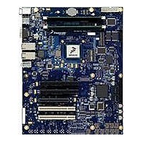
Manufacturer Part Number
MPC8572DS
Description
KIT MPU POWERQUICC III
Manufacturer
Freescale Semiconductor
Series
PowerQUICC III™r
Type
MPUr
Specifications of MPC8572DS
Contents
Board
Data Rate
10 Mbps to 100 Mbps
Memory Type
Flash, DDR, DDR2, DDR3, SDRAM
Interface Type
I2C, Ethernet
Operating Voltage
3.3 V
Data Bus Width
32 bit
Product
Development Tools
Silicon Manufacturer
Freescale
Core Architecture
Power Architecture
Core Sub-architecture
PowerQUICC
Silicon Core Number
MPC85xx
Silicon Family Name
PowerQUICC III
Rohs Compliant
Yes
For Use With/related Products
MPC8572E
Lead Free Status / RoHS Status
Lead free / RoHS Compliant


PCI Express
16.5
The RX eye diagram in
Figure
Note: In general, the minimum Receiver eye diagram measured with the compliance/test measurement
load (see
at the input Receiver of any real PCI Express component. The degraded eye diagram at the input Receiver
is due to traces internal to the package as well as silicon parasitic characteristics which cause the real PCI
Express component to vary in impedance from the compliance/test measurement load. The input Receiver
eye diagram is implementation specific and is not specified. RX component designer should provide
additional margin to adequately compensate for the degraded minimum Receiver eye diagram (shown in
Figure
the Return Loss measured looking into the RX package and silicon. The RX eye diagram must be aligned
in time using the jitter median to locate the center of the eye diagram.
The eye diagram must be valid for any 250 consecutive UIs.
A recovered TX UI is calculated over 3500 consecutive unit intervals of sample data. The eye diagram is
created using all edges of the 250 consecutive UI in the center of the 3500 UI used for calculating the TX
UI.
88
57) in place of any real PCI Express RX component.
56) expected at the input Receiver based on some adequate combination of system simulations and
Figure
Receiver Compliance Eye Diagrams
Figure 56. Minimum Receiver Eye Timing and Voltage Compliance Specification
The reference impedance for return loss measurements is 50. to ground for
both the D+ and D- line (that is, as measured by a Vector Network Analyzer
with 50. probes—see
optional for the return loss measurement.
MPC8572E PowerQUICC III Integrated Processor Hardware Specifications, Rev. 5
57) is larger than the minimum Receiver eye diagram measured over a range of systems
(D+ D– Crossing Point)
V
RX-DIFF
Figure 56
= 0 mV
is specified using the passive compliance/test measurement load (see
Figure
V
RX-DIFFp-p-MIN
57). Note that the series capacitors, CTX, are
0.4 UI = T
NOTE
RX-EYE-MIN
> 175 mV
(D+ D– Crossing Point)
V
RX-DIFF
= 0 mV
Freescale Semiconductor
Related parts for MPC8572DS
Image
Part Number
Description
Manufacturer
Datasheet
Request
R

Part Number:
Description:
Manufacturer:
Freescale Semiconductor, Inc
Datasheet:
Part Number:
Description:
Manufacturer:
Freescale Semiconductor, Inc
Datasheet:
Part Number:
Description:
Manufacturer:
Freescale Semiconductor, Inc
Datasheet:
Part Number:
Description:
Manufacturer:
Freescale Semiconductor, Inc
Datasheet:
Part Number:
Description:
Manufacturer:
Freescale Semiconductor, Inc
Datasheet:
Part Number:
Description:
Manufacturer:
Freescale Semiconductor, Inc
Datasheet:
Part Number:
Description:
Manufacturer:
Freescale Semiconductor, Inc
Datasheet:
Part Number:
Description:
Manufacturer:
Freescale Semiconductor, Inc
Datasheet:
Part Number:
Description:
Manufacturer:
Freescale Semiconductor, Inc
Datasheet:
Part Number:
Description:
Manufacturer:
Freescale Semiconductor, Inc
Datasheet:
Part Number:
Description:
Manufacturer:
Freescale Semiconductor, Inc
Datasheet:
Part Number:
Description:
Manufacturer:
Freescale Semiconductor, Inc
Datasheet:
Part Number:
Description:
Manufacturer:
Freescale Semiconductor, Inc
Datasheet:
Part Number:
Description:
Manufacturer:
Freescale Semiconductor, Inc
Datasheet:
Part Number:
Description:
Manufacturer:
Freescale Semiconductor, Inc
Datasheet: