MPC8572DS Freescale Semiconductor, MPC8572DS Datasheet - Page 82
MPC8572DS
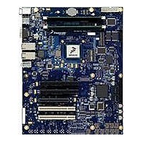
Manufacturer Part Number
MPC8572DS
Description
KIT MPU POWERQUICC III
Manufacturer
Freescale Semiconductor
Series
PowerQUICC III™r
Type
MPUr
Specifications of MPC8572DS
Contents
Board
Data Rate
10 Mbps to 100 Mbps
Memory Type
Flash, DDR, DDR2, DDR3, SDRAM
Interface Type
I2C, Ethernet
Operating Voltage
3.3 V
Data Bus Width
32 bit
Product
Development Tools
Silicon Manufacturer
Freescale
Core Architecture
Power Architecture
Core Sub-architecture
PowerQUICC
Silicon Core Number
MPC85xx
Silicon Family Name
PowerQUICC III
Rohs Compliant
Yes
For Use With/related Products
MPC8572E
Lead Free Status / RoHS Status
Lead free / RoHS Compliant


PCI Express
16.1
For more information, see
16.2
Table 61
16.3
The ports on the two ends of a link must transmit data at a rate that is within 600 parts per million (ppm)
of each other at all times. This is specified to allow bit rate clock sources with a +/– 300 ppm tolerance.
16.4
The following is a summary of the specifications for the physical layer of PCI Express on this device. For
further details as well as the specifications of the transport and data link layer, Use the PCI Express Base
Specification. REV. 1.0a document.
16.4.1
Table 62
specified at the component pins.
82
Notes:
1. Typical cycle time is based on PCI Express Card Electromechanical Specification Revision 1.0a.
UI
V
Symbol
t
t
TX-DIFFp-p
REFCJ
REFPJ
t
REF
Symbol
REFCLK cycle time
REFCLK cycle-to-cycle jitter. Difference in the period of any two adjacent
REFCLK cycles
Phase jitter. Deviation in edge location with respect to mean edge location
defines the specifications for the differential output at all transmitters (TXs). The parameters are
lists AC requirements.
DC Requirements for PCI Express SD1_REF_CLK and
AC Requirements for PCI Express SerDes Reference Clocks
SD1_REF_CLK
Clocking Dependencies
Physical Layer Specifications
Differential Transmitter (TX) Output
MPC8572E PowerQUICC III Integrated Processor Hardware Specifications, Rev. 5
Unit Interval
Differential
Peak-to-Peak
Output Voltage
Table 61. SD1_REF_CLK and SD1_REF_CLK AC Requirements
Parameter
Table 62. Differential Transmitter (TX) Output Specifications
Section 15.2, “SerDes Reference Clocks.”
Parameter Description
399.88
Min
0.8
Nominal
400
—
400.12
Max
1.2
Units
ps
V
Each UI is 400 ps ± 300 ppm. UI does not account
for Spread Spectrum Clock dictated variations. See
Note 1.
V
TX-DIFFp-p
= 2*|V
Min
–50
—
—
TX-D+
Typical
Comments
10
—
—
- V
Freescale Semiconductor
TX-D-
Max
100
50
—
| See Note 2.
Units Notes
ns
ps
ps
—
—
1
Related parts for MPC8572DS
Image
Part Number
Description
Manufacturer
Datasheet
Request
R

Part Number:
Description:
Manufacturer:
Freescale Semiconductor, Inc
Datasheet:
Part Number:
Description:
Manufacturer:
Freescale Semiconductor, Inc
Datasheet:
Part Number:
Description:
Manufacturer:
Freescale Semiconductor, Inc
Datasheet:
Part Number:
Description:
Manufacturer:
Freescale Semiconductor, Inc
Datasheet:
Part Number:
Description:
Manufacturer:
Freescale Semiconductor, Inc
Datasheet:
Part Number:
Description:
Manufacturer:
Freescale Semiconductor, Inc
Datasheet:
Part Number:
Description:
Manufacturer:
Freescale Semiconductor, Inc
Datasheet:
Part Number:
Description:
Manufacturer:
Freescale Semiconductor, Inc
Datasheet:
Part Number:
Description:
Manufacturer:
Freescale Semiconductor, Inc
Datasheet:
Part Number:
Description:
Manufacturer:
Freescale Semiconductor, Inc
Datasheet:
Part Number:
Description:
Manufacturer:
Freescale Semiconductor, Inc
Datasheet:
Part Number:
Description:
Manufacturer:
Freescale Semiconductor, Inc
Datasheet:
Part Number:
Description:
Manufacturer:
Freescale Semiconductor, Inc
Datasheet:
Part Number:
Description:
Manufacturer:
Freescale Semiconductor, Inc
Datasheet:
Part Number:
Description:
Manufacturer:
Freescale Semiconductor, Inc
Datasheet: