MPC8572DS Freescale Semiconductor, MPC8572DS Datasheet - Page 50
MPC8572DS
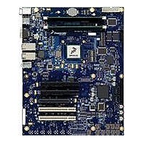
Manufacturer Part Number
MPC8572DS
Description
KIT MPU POWERQUICC III
Manufacturer
Freescale Semiconductor
Series
PowerQUICC III™r
Type
MPUr
Specifications of MPC8572DS
Contents
Board
Data Rate
10 Mbps to 100 Mbps
Memory Type
Flash, DDR, DDR2, DDR3, SDRAM
Interface Type
I2C, Ethernet
Operating Voltage
3.3 V
Data Bus Width
32 bit
Product
Development Tools
Silicon Manufacturer
Freescale
Core Architecture
Power Architecture
Core Sub-architecture
PowerQUICC
Silicon Core Number
MPC85xx
Silicon Family Name
PowerQUICC III
Rohs Compliant
Yes
For Use With/related Products
MPC8572E
Lead Free Status / RoHS Status
Lead free / RoHS Compliant


Ethernet Management Interface Electrical Characteristics
9
The electrical characteristics specified here apply to MII management interface signals ECn_MDIO
(management data input/output) and ECn_MDC (management data clock). The electrical characteristics
for GMII, SGMII, RGMII, RMII, TBI and RTBI are specified in
Three-Speed Ethernet (eTSEC).”
9.1
The ECn_MDC and ECn_MDIO are defined to operate at a supply voltage of 3.3 V or 2.5 V. The DC
electrical characteristics for ECn_MDIO and ECn_MDC are provided in
50
At recommended operating conditions with LV
TSEC_1588_CLK_OUT duty cycle
TSEC_1588_PULSE_OUT
TSEC_1588_TRIG_IN pulse width
Note:
1.When TMR_CTRL[CKSEL] is set as ‘00’, the external TSEC_1588_CLK input is selected as the 1588 timer reference clock
2. It needs to be at least two times of the clock period of the clock selected by TMR_CTRL[CKSEL].
source, with the timing defined in
is defined in terms of T
port is running at. When eTSEC1 is configured to operate in the parallel mode, the T
of the TSEC1_TX_CLK. When eTSEC1 operates in SGMII mode, the maximum value of t
the recovered clock from SGMII SerDes. For example, for SGMII 10/100/1000 Mbps modes, the maximum value of
t
Reference Manual for detailed description of TMR_CTRL registers.
Supply voltage (3.3 V)
Output high voltage
(LV
Output low voltage
(LV
Input high voltage
Input low voltage
Input high current
(LV
T1588CLK
DD
DD
DD
Ethernet Management Interface Electrical
Characteristics
/TV
/TV
/TV
Parameter/Condition
MII Management DC Electrical Characteristics
DD
DD
DD
is 3600, 360, 72 ns respectively. See the MPC8572E PowerQUICC™ III Integrated Communications Processor
Parameter
= Min, I
=Min, I
= Max, V
Table 43. MII Management DC Electrical Characteristics (LV
MPC8572E PowerQUICC III Integrated Processor Hardware Specifications, Rev. 5
OL
OH
Table 42. eTSEC IEEE 1588 AC Timing Specifications (continued)
IN
= 1.0 mA)
TX_CLK
= –1.0 mA)
3
= 2.1 V)
, that is the maximum clock cycle period of the equivalent interface speed that the eTSEC1
Table
DD
LV
42, “eTSEC IEEE 1588 AC Timing Specifications.” The maximum value of t
Symbol
/TV
DD
V
V
V
V
I
OH
IH
DD
/TV
OL
/t
IH
IL
t
T1588CLKOTH
t
T1588CLKOUT
T1588TRIGH
of 3.3 V ± 5% or 2.5 V ± 5%
t
Symbol
DD
T1588OV
GND
3.13
2.10
Min
2.0
—
—
2*t
T1588CLK_MAX
Min
0.5
30
“Section 8, “Ethernet: Enhanced
OV
DD
Max
3.47
0.50
0.90
40
Typ
—
50
—
—
+ 0.3
Table 43
TX_CLK
DD
/TV
T1588CLK
is the maximum clock period
DD
Max
3.0
70
—
=3.3 V)
and
Unit
μA
Freescale Semiconductor
V
V
V
V
V
is defined in terms of
Table
Unit
ns
ns
%
44.
Notes
1, 2
—
—
—
—
—
T1588CLK
Note
—
—
2
Related parts for MPC8572DS
Image
Part Number
Description
Manufacturer
Datasheet
Request
R

Part Number:
Description:
Manufacturer:
Freescale Semiconductor, Inc
Datasheet:
Part Number:
Description:
Manufacturer:
Freescale Semiconductor, Inc
Datasheet:
Part Number:
Description:
Manufacturer:
Freescale Semiconductor, Inc
Datasheet:
Part Number:
Description:
Manufacturer:
Freescale Semiconductor, Inc
Datasheet:
Part Number:
Description:
Manufacturer:
Freescale Semiconductor, Inc
Datasheet:
Part Number:
Description:
Manufacturer:
Freescale Semiconductor, Inc
Datasheet:
Part Number:
Description:
Manufacturer:
Freescale Semiconductor, Inc
Datasheet:
Part Number:
Description:
Manufacturer:
Freescale Semiconductor, Inc
Datasheet:
Part Number:
Description:
Manufacturer:
Freescale Semiconductor, Inc
Datasheet:
Part Number:
Description:
Manufacturer:
Freescale Semiconductor, Inc
Datasheet:
Part Number:
Description:
Manufacturer:
Freescale Semiconductor, Inc
Datasheet:
Part Number:
Description:
Manufacturer:
Freescale Semiconductor, Inc
Datasheet:
Part Number:
Description:
Manufacturer:
Freescale Semiconductor, Inc
Datasheet:
Part Number:
Description:
Manufacturer:
Freescale Semiconductor, Inc
Datasheet:
Part Number:
Description:
Manufacturer:
Freescale Semiconductor, Inc
Datasheet: