MPC8572DS Freescale Semiconductor, MPC8572DS Datasheet - Page 12
MPC8572DS
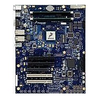
Manufacturer Part Number
MPC8572DS
Description
KIT MPU POWERQUICC III
Manufacturer
Freescale Semiconductor
Series
PowerQUICC III™r
Type
MPUr
Specifications of MPC8572DS
Contents
Board
Data Rate
10 Mbps to 100 Mbps
Memory Type
Flash, DDR, DDR2, DDR3, SDRAM
Interface Type
I2C, Ethernet
Operating Voltage
3.3 V
Data Bus Width
32 bit
Product
Development Tools
Silicon Manufacturer
Freescale
Core Architecture
Power Architecture
Core Sub-architecture
PowerQUICC
Silicon Core Number
MPC85xx
Silicon Family Name
PowerQUICC III
Rohs Compliant
Yes
For Use With/related Products
MPC8572E
Lead Free Status / RoHS Status
Lead free / RoHS Compliant


Electrical Characteristics
2.1.2
Table 2
recommended and tested operating conditions. Proper device operation outside these conditions is not
guaranteed.
12
Core supply voltage
PLL supply voltage
Core power supply for SerDes transceivers
Pad power supply for SerDes transceivers
DDR SDRAM
Controller I/O
supply voltage
Three-speed Ethernet I/O voltage
Local bus and GPIO I/O voltage
Input voltage
Junction temperature range
Notes:
1. This voltage is the input to the filter discussed in
2. Caution: MV
3. Caution: OV
4. Caution: L/TV
DUART, system control and power management, I
voltage at the AV
power-on reset and power-down sequences.
power-on reset and power-down sequences.
power-on reset and power-down sequences.
provides the recommended operating conditions for this device. Note that the values shown are the
Recommended Operating Conditions
IN
IN
IN
must not exceed OV
must not exceed GV
MPC8572E PowerQUICC III Integrated Processor Hardware Specifications, Rev. 5
must not exceed L/TV
DD
DDR2 SDRAM Interface
DDR3 SDRAM Interface
DDR2 and DDR3 SDRAM Interface signals
DDR2 and DDR3 SDRAM Interface reference
Three-speed Ethernet signals
Local bus and GPIO signals
Local bus, DUART, SYSCLK, Serial RapidIO, system
control and power management, I
signals
pin, that may be reduced from V
Characteristic
Table 2. Recommended Operating Conditions
DD
DD
DD
by more than 0.3 V. This limit may be exceeded for a maximum of 20 ms during
by more than 0.3 V. This limit may be exceeded for a maximum of 20 ms during
by more than 0.3 V. This limit may be exceeded for a maximum of 20 ms during
2
C, and JTAG I/O voltage
Section 21.2.1, “PLL Power Supply Filtering,”
DD
2
C, and JTAG
by the filter.
MV
Symbol Recommended Value Unit Notes
SV
XV
GV
OV
BV
AV
TV
LV
MV
OV
BV
TV
V
LV
T
REF
DD
DD
DD
DD
DD
DD
DD
DD
DD
IN
J
IN
IN
IN
IN
n
3.3 V ± 165 mV
2.5 V ± 125 mV
3.3 V ± 165 mV
2.5 V ± 125 mV
3.3 V ± 165 mV
3.3 V ± 165 mV
2.5 V ± 125 mV
1.1 V ± 55 mV
1.1 V ± 55 mV
1.1 V ± 55 mV
1.1 V ± 55 mV
1.8 V ± 90 mV
1.5 V ± 75 mV
1.8 V ± 90 mV
GND to GV
GND to OV
GND to TV
GND to BV
GV
GND to LV
0 to 105
DD
and not necessarily the
/2 ± 1%
Freescale Semiconductor
DD
DD
DD
DD
DD
°C
V
V
V
V
V
V
V
V
V
V
V
V
V
—
—
—
—
—
—
—
—
—
1
4
4
3
2
4
3
Related parts for MPC8572DS
Image
Part Number
Description
Manufacturer
Datasheet
Request
R

Part Number:
Description:
Manufacturer:
Freescale Semiconductor, Inc
Datasheet:
Part Number:
Description:
Manufacturer:
Freescale Semiconductor, Inc
Datasheet:
Part Number:
Description:
Manufacturer:
Freescale Semiconductor, Inc
Datasheet:
Part Number:
Description:
Manufacturer:
Freescale Semiconductor, Inc
Datasheet:
Part Number:
Description:
Manufacturer:
Freescale Semiconductor, Inc
Datasheet:
Part Number:
Description:
Manufacturer:
Freescale Semiconductor, Inc
Datasheet:
Part Number:
Description:
Manufacturer:
Freescale Semiconductor, Inc
Datasheet:
Part Number:
Description:
Manufacturer:
Freescale Semiconductor, Inc
Datasheet:
Part Number:
Description:
Manufacturer:
Freescale Semiconductor, Inc
Datasheet:
Part Number:
Description:
Manufacturer:
Freescale Semiconductor, Inc
Datasheet:
Part Number:
Description:
Manufacturer:
Freescale Semiconductor, Inc
Datasheet:
Part Number:
Description:
Manufacturer:
Freescale Semiconductor, Inc
Datasheet:
Part Number:
Description:
Manufacturer:
Freescale Semiconductor, Inc
Datasheet:
Part Number:
Description:
Manufacturer:
Freescale Semiconductor, Inc
Datasheet:
Part Number:
Description:
Manufacturer:
Freescale Semiconductor, Inc
Datasheet: