MPC8572DS Freescale Semiconductor, MPC8572DS Datasheet - Page 71
MPC8572DS
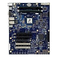
Manufacturer Part Number
MPC8572DS
Description
KIT MPU POWERQUICC III
Manufacturer
Freescale Semiconductor
Series
PowerQUICC III™r
Type
MPUr
Specifications of MPC8572DS
Contents
Board
Data Rate
10 Mbps to 100 Mbps
Memory Type
Flash, DDR, DDR2, DDR3, SDRAM
Interface Type
I2C, Ethernet
Operating Voltage
3.3 V
Data Bus Width
32 bit
Product
Development Tools
Silicon Manufacturer
Freescale
Core Architecture
Power Architecture
Core Sub-architecture
PowerQUICC
Silicon Core Number
MPC85xx
Silicon Family Name
PowerQUICC III
Rohs Compliant
Yes
For Use With/related Products
MPC8572E
Lead Free Status / RoHS Status
Lead free / RoHS Compliant


14.2
Table 59
Figure 42
15 High-Speed Serial Interfaces (HSSI)
The MPC8572E features two Serializer/Deserializer (SerDes) interfaces to be used for high-speed serial
interconnect applications. The SerDes1 interface can be used for PCI Express and/or Serial RapidIO data
transfers. The SerDes2 is dedicated for SGMII application.
This section describes the common portion of SerDes DC electrical specifications, which is the DC
requirement for SerDes Reference Clocks. The SerDes data lane’s transmitter and receiver reference
circuits are also shown.
15.1
The SerDes utilizes differential signaling to transfer data across the serial link. This section defines terms
used in the description and specification of differential signals.
Figure 43
description. The figure shows waveform for either a transmitter output (SDn_TX and SDn_TX) or a
receiver input (SDn_RX and SDn_RX). Each signal swings between A Volts and B Volts where A > B.
Using this waveform, the definitions are as follows. To simplify illustration, the following definitions
assume that the SerDes transmitter and receiver operate in a fully symmetrical differential signaling
environment.
Freescale Semiconductor
GPIO inputs—minimum pulse width
Notes:
1. Input specifications are measured from the 50% level of the signal to the 50% level of the rising edge of SYSCLK. Timings
2. GPIO inputs and outputs are asynchronous to any visible clock. GPIO outputs should be synchronized before use by any
are measured at the pin.
external synchronous logic. GPIO inputs are required to be valid for at least t
1. Single-Ended Swing
The transmitter output signals and the receiver input signals SDn_TX, SDn_TX, SDn_RX and
SDn_RX each have a peak-to-peak swing of A - B Volts. This is also referred as each signal wire’s
Single-Ended Swing.
provides the GPIO input and output AC timing specifications.
GPIO AC Electrical Specifications
Signal Terms Definition
provides the AC test load for the GPIO.
shows how the signals are defined. For illustration purpose, only one SerDes lane is used for
MPC8572E PowerQUICC III Integrated Processor Hardware Specifications, Rev. 5
Output
Parameter
Table 59. GPIO Input AC Timing Specifications
Figure 42. GPIO AC Test Load
Z
0
= 50 Ω
R
L
= 50 Ω
PIWID
Symbol
t
PIWID
ns to ensure proper operation.
1
BV
High-Speed Serial Interfaces (HSSI)
DD
/2
Typ
20
Unit
ns
Notes
2
71
Related parts for MPC8572DS
Image
Part Number
Description
Manufacturer
Datasheet
Request
R

Part Number:
Description:
Manufacturer:
Freescale Semiconductor, Inc
Datasheet:
Part Number:
Description:
Manufacturer:
Freescale Semiconductor, Inc
Datasheet:
Part Number:
Description:
Manufacturer:
Freescale Semiconductor, Inc
Datasheet:
Part Number:
Description:
Manufacturer:
Freescale Semiconductor, Inc
Datasheet:
Part Number:
Description:
Manufacturer:
Freescale Semiconductor, Inc
Datasheet:
Part Number:
Description:
Manufacturer:
Freescale Semiconductor, Inc
Datasheet:
Part Number:
Description:
Manufacturer:
Freescale Semiconductor, Inc
Datasheet:
Part Number:
Description:
Manufacturer:
Freescale Semiconductor, Inc
Datasheet:
Part Number:
Description:
Manufacturer:
Freescale Semiconductor, Inc
Datasheet:
Part Number:
Description:
Manufacturer:
Freescale Semiconductor, Inc
Datasheet:
Part Number:
Description:
Manufacturer:
Freescale Semiconductor, Inc
Datasheet:
Part Number:
Description:
Manufacturer:
Freescale Semiconductor, Inc
Datasheet:
Part Number:
Description:
Manufacturer:
Freescale Semiconductor, Inc
Datasheet:
Part Number:
Description:
Manufacturer:
Freescale Semiconductor, Inc
Datasheet:
Part Number:
Description:
Manufacturer:
Freescale Semiconductor, Inc
Datasheet: