MPC8572DS Freescale Semiconductor, MPC8572DS Datasheet - Page 33
MPC8572DS
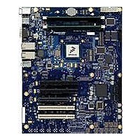
Manufacturer Part Number
MPC8572DS
Description
KIT MPU POWERQUICC III
Manufacturer
Freescale Semiconductor
Series
PowerQUICC III™r
Type
MPUr
Specifications of MPC8572DS
Contents
Board
Data Rate
10 Mbps to 100 Mbps
Memory Type
Flash, DDR, DDR2, DDR3, SDRAM
Interface Type
I2C, Ethernet
Operating Voltage
3.3 V
Data Bus Width
32 bit
Product
Development Tools
Silicon Manufacturer
Freescale
Core Architecture
Power Architecture
Core Sub-architecture
PowerQUICC
Silicon Core Number
MPC85xx
Silicon Family Name
PowerQUICC III
Rohs Compliant
Yes
For Use With/related Products
MPC8572E
Lead Free Status / RoHS Status
Lead free / RoHS Compliant


Figure 9
8.2.2.2
Table 28
Figure 10
Freescale Semiconductor
At recommended operating conditions with LV
RX_CLK clock period
RX_CLK duty cycle
RXD[7:0], RX_DV, RX_ER setup time to RX_CLK
RXD[7:0], RX_DV, RX_ER hold time to RX_CLK
RX_CLK clock rise (20%-80%)
RX_CLK clock fall time (80%-20%)
Note:
1. The symbols used for timing specifications herein follow the pattern of t
2. Guaranteed by design.
for inputs and t
receive timing (GR) with respect to the time data input signals (D) reaching the valid state (V) relative to the t
reference (K) going to the high state (H) or setup time. Also, t
the time data input signals (D) went invalid (X) relative to the t
Note that, in general, the clock reference symbol representation is based on three letters representing the clock of a particular
functional. For example, the subscript of t
convention is used with the appropriate letter: R (rise) or F (fall).
shows the GMII transmit AC timing diagram.
provides the GMII receive AC timing specifications.
provides the AC test load for eTSEC.
GMII Receive AC Timing Specifications
(first two letters of functional block)(reference)(state)(signal)(state)
GTX_CLK
Parameter/Condition
MPC8572E PowerQUICC III Integrated Processor Hardware Specifications, Rev. 5
TXD[7:0]
TX_EN
TX_ER
Output
Table 28. GMII Receive AC Timing Specifications
Figure 9. GMII Transmit AC Timing Diagram
t
tG
GTXH
DD
TKHDV
/TV
GRX
Figure 10. eTSEC AC Test Load
DD
t
GTX
Z
represents the GMII (G) receive (RX) clock. For rise and fall times, the latter
of 2.5/ 3.3 V ± 5%.
0
= 50 Ω
t
GRX
GRDXKL
Symbol
GRXH
t
t
t
GRDVKH
GRDXKH
t
t
GTXF
GRXR
GRXF
t
GRX
clock reference (K) going to the low (L) state or hold time.
/t
t
GTKHDX
GRX
2
2
for outputs. For example, t
symbolizes GMII receive timing (GR) with respect to
(first two letters of functional block)(signal)(state) (reference)(state)
1
R
Ethernet: Enhanced Three-Speed Ethernet (eTSEC)
L
t
GTXR
= 50 Ω
Min
2.0
40
—
—
—
0
LV
DD
Typ
8.0
—
—
—
—
—
/2
GRDVKH
symbolizes GMII
Max
1.0
1.0
60
—
—
—
RX
clock
Unit
ns
ns
ns
ns
ns
ns
33
Related parts for MPC8572DS
Image
Part Number
Description
Manufacturer
Datasheet
Request
R

Part Number:
Description:
Manufacturer:
Freescale Semiconductor, Inc
Datasheet:
Part Number:
Description:
Manufacturer:
Freescale Semiconductor, Inc
Datasheet:
Part Number:
Description:
Manufacturer:
Freescale Semiconductor, Inc
Datasheet:
Part Number:
Description:
Manufacturer:
Freescale Semiconductor, Inc
Datasheet:
Part Number:
Description:
Manufacturer:
Freescale Semiconductor, Inc
Datasheet:
Part Number:
Description:
Manufacturer:
Freescale Semiconductor, Inc
Datasheet:
Part Number:
Description:
Manufacturer:
Freescale Semiconductor, Inc
Datasheet:
Part Number:
Description:
Manufacturer:
Freescale Semiconductor, Inc
Datasheet:
Part Number:
Description:
Manufacturer:
Freescale Semiconductor, Inc
Datasheet:
Part Number:
Description:
Manufacturer:
Freescale Semiconductor, Inc
Datasheet:
Part Number:
Description:
Manufacturer:
Freescale Semiconductor, Inc
Datasheet:
Part Number:
Description:
Manufacturer:
Freescale Semiconductor, Inc
Datasheet:
Part Number:
Description:
Manufacturer:
Freescale Semiconductor, Inc
Datasheet:
Part Number:
Description:
Manufacturer:
Freescale Semiconductor, Inc
Datasheet:
Part Number:
Description:
Manufacturer:
Freescale Semiconductor, Inc
Datasheet: