MPC8572DS Freescale Semiconductor, MPC8572DS Datasheet - Page 2
MPC8572DS
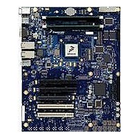
Manufacturer Part Number
MPC8572DS
Description
KIT MPU POWERQUICC III
Manufacturer
Freescale Semiconductor
Series
PowerQUICC III™r
Type
MPUr
Specifications of MPC8572DS
Contents
Board
Data Rate
10 Mbps to 100 Mbps
Memory Type
Flash, DDR, DDR2, DDR3, SDRAM
Interface Type
I2C, Ethernet
Operating Voltage
3.3 V
Data Bus Width
32 bit
Product
Development Tools
Silicon Manufacturer
Freescale
Core Architecture
Power Architecture
Core Sub-architecture
PowerQUICC
Silicon Core Number
MPC85xx
Silicon Family Name
PowerQUICC III
Rohs Compliant
Yes
For Use With/related Products
MPC8572E
Lead Free Status / RoHS Status
Lead free / RoHS Compliant


Overview
2
•
•
•
— Embedded vector and scalar single-precision floating-point APUs. Provide an instruction set
— Double-precision floating-point APU. Provides an instruction set for double-precision (64-bit)
— 36-bit real addressing
— Memory management unit (MMU). Especially designed for embedded applications. Supports
— Enhanced hardware and software debug support
— Performance monitor facility that is similar to, but separate from, the MPC8572E performance
The e500 defines features that are not implemented on this device. It also generally defines some
features that this device implements more specifically. An understanding of these differences can
be critical to ensure proper operation.
1 Mbyte L2 cache/SRAM
— Shared by both cores.
— Flexible configuration and individually configurable per core.
— Full ECC support on 64-bit boundary in both cache and SRAM modes
— Cache mode supports instruction caching, data caching, or both.
— External masters can force data to be allocated into the cache through programmed memory
— Eight-way set-associative cache organization (32-byte cache lines)
— Supports locking entire cache or selected lines. Individual line locks are set and cleared through
— Global locking and Flash clearing done through writes to L2 configuration registers
— Instruction and data locks can be Flash cleared separately.
— Per-way allocation of cache region to a given processor.
— SRAM features include the following:
e500 coherency module (ECM) manages core and intrasystem transactions
Address translation and mapping unit (ATMU)
— Twelve local access windows define mapping within local 36-bit address space.
— Inbound and outbound ATMUs map to larger external address spaces.
the upper and lower words of the 64-bit GPRs as they are defined by the SPE APU.
for single-precision (32-bit) floating-point instructions.
floating-point instructions that use the 64-bit GPRs.
4-Kbyte to 4-Gbyte page sizes.
monitor
ranges or special transaction types (stashing).
– 1, 2, or 4 ways can be configured for stashing only.
Book E instructions or by externally mastered transactions.
– 1, 2, 4, or 8 ways can be configured as SRAM.
– I/O devices access SRAM regions by marking transactions as snoopable (global).
– Regions can reside at any aligned location in the memory map.
– Byte-accessible ECC is protected using read-modify-write transaction accesses for
– Three inbound windows plus a configuration window on PCI Express
smaller-than-cache-line accesses.
MPC8572E PowerQUICC III Integrated Processor Hardware Specifications, Rev. 5
Freescale Semiconductor
Related parts for MPC8572DS
Image
Part Number
Description
Manufacturer
Datasheet
Request
R

Part Number:
Description:
Manufacturer:
Freescale Semiconductor, Inc
Datasheet:
Part Number:
Description:
Manufacturer:
Freescale Semiconductor, Inc
Datasheet:
Part Number:
Description:
Manufacturer:
Freescale Semiconductor, Inc
Datasheet:
Part Number:
Description:
Manufacturer:
Freescale Semiconductor, Inc
Datasheet:
Part Number:
Description:
Manufacturer:
Freescale Semiconductor, Inc
Datasheet:
Part Number:
Description:
Manufacturer:
Freescale Semiconductor, Inc
Datasheet:
Part Number:
Description:
Manufacturer:
Freescale Semiconductor, Inc
Datasheet:
Part Number:
Description:
Manufacturer:
Freescale Semiconductor, Inc
Datasheet:
Part Number:
Description:
Manufacturer:
Freescale Semiconductor, Inc
Datasheet:
Part Number:
Description:
Manufacturer:
Freescale Semiconductor, Inc
Datasheet:
Part Number:
Description:
Manufacturer:
Freescale Semiconductor, Inc
Datasheet:
Part Number:
Description:
Manufacturer:
Freescale Semiconductor, Inc
Datasheet:
Part Number:
Description:
Manufacturer:
Freescale Semiconductor, Inc
Datasheet:
Part Number:
Description:
Manufacturer:
Freescale Semiconductor, Inc
Datasheet:
Part Number:
Description:
Manufacturer:
Freescale Semiconductor, Inc
Datasheet: