MPC8572DS Freescale Semiconductor, MPC8572DS Datasheet - Page 39
MPC8572DS
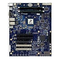
Manufacturer Part Number
MPC8572DS
Description
KIT MPU POWERQUICC III
Manufacturer
Freescale Semiconductor
Series
PowerQUICC III™r
Type
MPUr
Specifications of MPC8572DS
Contents
Board
Data Rate
10 Mbps to 100 Mbps
Memory Type
Flash, DDR, DDR2, DDR3, SDRAM
Interface Type
I2C, Ethernet
Operating Voltage
3.3 V
Data Bus Width
32 bit
Product
Development Tools
Silicon Manufacturer
Freescale
Core Architecture
Power Architecture
Core Sub-architecture
PowerQUICC
Silicon Core Number
MPC85xx
Silicon Family Name
PowerQUICC III
Rohs Compliant
Yes
For Use With/related Products
MPC8572E
Lead Free Status / RoHS Status
Lead free / RoHS Compliant


Figure 17
8.2.6
Table 34
At recommended operating conditions with LV
Freescale Semiconductor
Data to clock output skew (at transmitter)
Data to clock input skew (at receiver)
Clock period
Duty cycle for 10BASE-T and 100BASE-TX
Rise time (20%–80%)
Fall time (20%–80%)
Notes:
1. Note that, in general, the clock reference symbol representation for this section is based on the symbols RGT to represent
2. This implies that PC board design requires clocks to be routed such that an additional trace delay of greater than 1.5 ns will
3. For 10 and 100 Mbps, t
4. Duty cycle may be stretched/shrunk during speed changes or while transitioning to a received packet's clock domains as long
RGMII and RTBI timing. For example, the subscript of t
notation for rise (R) and fall (F) times follows the clock symbol that is being represented. For symbols representing skews, the
subscript is skew (SK) followed by the clock that is being skewed (RGT).
be added to the associated clock signal.
as the minimum duty cycle is not violated and stretching occurs for no more than three t
between.
presents the RGMII and RTBI AC timing specifications.
RX_CLK
RCG[9:0]
shows the TBI receive the timing diagram.
3
RGMII and RTBI AC Timing
Parameter/Condition
MPC8572E PowerQUICC III Integrated Processor Hardware Specifications, Rev. 5
Figure 17. TBI Single-Clock Mode Receive AC Timing Diagram
RGT
scales to 400 ns ± 40 ns and 40 ns ± 4 ns, respectively.
t
TRRH
Table 34. RGMII and RTBI AC Timing Specifications
2
DD
t
/TV
TRR
3, 4
DD
of 2.5 V ± 5%.
t
TRRDV
valid data
t
Symbol
RGTH
RGT
t
t
t
SKRGT
SKRGT
t
Specifications
t
RGTR
RGTF
RGT
represents the TBI (T) receive (RX) clock. Note also that the
/t
t
TRRDX
RGT
1
–500
Min
1.0
7.2
t
40
—
—
Ethernet: Enhanced Three-Speed Ethernet (eTSEC)
TRRF
RGT
Typ
8.0
—
50
—
—
0
of the lowest speed transitioned
t
TRRR
Max
0.75
0.75
500
2.8
8.8
60
Unit
ps
ns
ns
ns
ns
%
39
Related parts for MPC8572DS
Image
Part Number
Description
Manufacturer
Datasheet
Request
R

Part Number:
Description:
Manufacturer:
Freescale Semiconductor, Inc
Datasheet:
Part Number:
Description:
Manufacturer:
Freescale Semiconductor, Inc
Datasheet:
Part Number:
Description:
Manufacturer:
Freescale Semiconductor, Inc
Datasheet:
Part Number:
Description:
Manufacturer:
Freescale Semiconductor, Inc
Datasheet:
Part Number:
Description:
Manufacturer:
Freescale Semiconductor, Inc
Datasheet:
Part Number:
Description:
Manufacturer:
Freescale Semiconductor, Inc
Datasheet:
Part Number:
Description:
Manufacturer:
Freescale Semiconductor, Inc
Datasheet:
Part Number:
Description:
Manufacturer:
Freescale Semiconductor, Inc
Datasheet:
Part Number:
Description:
Manufacturer:
Freescale Semiconductor, Inc
Datasheet:
Part Number:
Description:
Manufacturer:
Freescale Semiconductor, Inc
Datasheet:
Part Number:
Description:
Manufacturer:
Freescale Semiconductor, Inc
Datasheet:
Part Number:
Description:
Manufacturer:
Freescale Semiconductor, Inc
Datasheet:
Part Number:
Description:
Manufacturer:
Freescale Semiconductor, Inc
Datasheet:
Part Number:
Description:
Manufacturer:
Freescale Semiconductor, Inc
Datasheet:
Part Number:
Description:
Manufacturer:
Freescale Semiconductor, Inc
Datasheet: