MPC8572DS Freescale Semiconductor, MPC8572DS Datasheet - Page 80
MPC8572DS
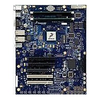
Manufacturer Part Number
MPC8572DS
Description
KIT MPU POWERQUICC III
Manufacturer
Freescale Semiconductor
Series
PowerQUICC III™r
Type
MPUr
Specifications of MPC8572DS
Contents
Board
Data Rate
10 Mbps to 100 Mbps
Memory Type
Flash, DDR, DDR2, DDR3, SDRAM
Interface Type
I2C, Ethernet
Operating Voltage
3.3 V
Data Bus Width
32 bit
Product
Development Tools
Silicon Manufacturer
Freescale
Core Architecture
Power Architecture
Core Sub-architecture
PowerQUICC
Silicon Core Number
MPC85xx
Silicon Family Name
PowerQUICC III
Rohs Compliant
Yes
For Use With/related Products
MPC8572E
Lead Free Status / RoHS Status
Lead free / RoHS Compliant


High-Speed Serial Interfaces (HSSI)
occurs in the 1-15MHz range. The source impedance of the clock driver should be 50 ohms to match the
transmission line and reduce reflections which are a source of noise to the system.
Table 60
80
At recommended operating conditions with XV
Rising Edge Rate
Falling Edge Rate
Differential Input High Voltage
Differential Input Low Voltage
Rising edge rate (SDn_REF_CLK) to falling edge rate
(SDn_REF_CLK) matching
Notes:
1. Measurement taken from single ended waveform.
2. Measurement taken from differential waveform.
3. Measured from -200 mV to +200 mV on the differential waveform (derived from SDn_REF_CLK minus SDn_REF_CLK). The
signal must be monotonic through the measurement region for rise and fall time. The 400 mV measurement window is centered
on the differential zero crossing. See
4. Matching applies to rising edge rate for SDn_REF_CLK and falling edge rate for SDn_REF_CLK. It is measured using a 200
mV window centered on the median cross point where SDn_REF_CLK rising meets SDn_REF_CLK falling. The median cross
point is used to calculate the voltage thresholds the oscilloscope is to use for the edge rate calculations. The Rise Edge Rate
of SDn_REF_CLK should be compared to the Fall Edge Rate of SDn_REF_CLK, the maximum allowed difference should not
exceed 20% of the slowest edge rate. See
V
V
SD_REF_CLK
SD_REF_CLK
IH
IL
= –200 mV
= +200 mV
describes some AC parameters common to SGMII, PCI Express and Serial RapidIO protocols.
0.0 V
SD n _REF_CLK
SD n _REF_CLK
Figure 53. Single-Ended Measurement Points for Rise and Fall Time Matching
–
MPC8572E PowerQUICC III Integrated Processor Hardware Specifications, Rev. 5
Figure 52. Differential Measurement Points for Rise and Fall Time
Parameter
Table 60. SerDes Reference Clock Common AC Parameters
Rise Edge Rate
Figure
DD_SRDS1
Figure
52.
or XV
53.
DD_SRDS2
= 1.1V ± 5%.
Rise Edge Rate
Fall Edge Rate
SD n _REF_CLK
SD n _REF_CLK
Matching
Rise-Fall
Symbol
V
V
IH
IL
Fall Edge Rate
+200
Min
1.0
1.0
—
—
Max
-200
4.0
4.0
20
Freescale Semiconductor
V/ns
V/ns
Unit
mV
mV
%
Notes
2, 3
2, 3
1, 4
2
2
Related parts for MPC8572DS
Image
Part Number
Description
Manufacturer
Datasheet
Request
R

Part Number:
Description:
Manufacturer:
Freescale Semiconductor, Inc
Datasheet:
Part Number:
Description:
Manufacturer:
Freescale Semiconductor, Inc
Datasheet:
Part Number:
Description:
Manufacturer:
Freescale Semiconductor, Inc
Datasheet:
Part Number:
Description:
Manufacturer:
Freescale Semiconductor, Inc
Datasheet:
Part Number:
Description:
Manufacturer:
Freescale Semiconductor, Inc
Datasheet:
Part Number:
Description:
Manufacturer:
Freescale Semiconductor, Inc
Datasheet:
Part Number:
Description:
Manufacturer:
Freescale Semiconductor, Inc
Datasheet:
Part Number:
Description:
Manufacturer:
Freescale Semiconductor, Inc
Datasheet:
Part Number:
Description:
Manufacturer:
Freescale Semiconductor, Inc
Datasheet:
Part Number:
Description:
Manufacturer:
Freescale Semiconductor, Inc
Datasheet:
Part Number:
Description:
Manufacturer:
Freescale Semiconductor, Inc
Datasheet:
Part Number:
Description:
Manufacturer:
Freescale Semiconductor, Inc
Datasheet:
Part Number:
Description:
Manufacturer:
Freescale Semiconductor, Inc
Datasheet:
Part Number:
Description:
Manufacturer:
Freescale Semiconductor, Inc
Datasheet:
Part Number:
Description:
Manufacturer:
Freescale Semiconductor, Inc
Datasheet: