MPC8572DS Freescale Semiconductor, MPC8572DS Datasheet - Page 126
MPC8572DS
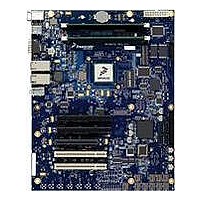
Manufacturer Part Number
MPC8572DS
Description
KIT MPU POWERQUICC III
Manufacturer
Freescale Semiconductor
Series
PowerQUICC III™r
Type
MPUr
Specifications of MPC8572DS
Contents
Board
Data Rate
10 Mbps to 100 Mbps
Memory Type
Flash, DDR, DDR2, DDR3, SDRAM
Interface Type
I2C, Ethernet
Operating Voltage
3.3 V
Data Bus Width
32 bit
Product
Development Tools
Silicon Manufacturer
Freescale
Core Architecture
Power Architecture
Core Sub-architecture
PowerQUICC
Silicon Core Number
MPC85xx
Silicon Family Name
PowerQUICC III
Rohs Compliant
Yes
For Use With/related Products
MPC8572E
Lead Free Status / RoHS Status
Lead free / RoHS Compliant


System Design Information
21.5
To ensure reliable operation, it is highly recommended to connect unused inputs to an appropriate signal
level. All unused active low inputs should be tied to V
required. All unused active high inputs should be connected to GND. All NC (no-connect) signals must
remain unconnected. Power and ground connections must be made to all external V
OV
21.6
The MPC8572E requires weak pull-up resistors (2–10 kΩ is recommended) on open drain type pins
including I
Correct operation of the JTAG interface requires configuration of a group of system control pins as
demonstrated in
state under normal operating conditions as most have asynchronous behavior and spurious assertion gives
unpredictable results.
The following pins must NOT be pulled down during power-on reset: DMA_DACK[0:1], EC5_MDC,
HRESET_REQ, TRIG_OUT/READY_P0/QUIESCE, MSRCID[2:4], MDVAL, and ASLEEP. The
TEST_SEL pin must be set to a proper state during POR configuration. For more details, refer to the pinlist
table of the individual device.
21.7
The MPC8572E drivers are characterized over process, voltage, and temperature. For all buses, the driver
is a push-pull single-ended driver type (open drain for I
To measure Z
or GND. Then, the value of each resistor is varied until the pad voltage is OV
output impedance is the average of two components, the resistances of the pull-up and pull-down devices.
When data is held high, SW1 is closed (SW2 is open) and R
OV
other in value. Then, Z
126
DD
DD
•
•
•
, GV
/2. R
First, the board should have at least 10 x 10-nF SMT ceramic chip capacitors as close as possible
to the supply balls of the device. Where the board has blind vias, these capacitors should be placed
directly below the chip supply and ground connections. Where the board does not have blind vias,
these capacitors should be placed in a ring around the device as close to the supply and ground
connections as possible.
Second, there should be a 1-µF ceramic chip capacitor from each SerDes supply (SV
and XV
all SerDes supplies.
Third, between the device and any SerDes voltage regulator there should be a 10-µF, low
equivalent series resistance (ESR) SMT tantalum chip capacitor and a 100-µF, low ESR SMT
tantalum chip capacitor. This should be done for all SerDes supplies.
Connection Recommendations
Pull-Up and Pull-Down Resistor Requirements
Output Buffer DC Impedance
2
P
DD
C pins and MPIC interrupt pins.
then becomes the resistance of the pull-up devices. R
0
, and LV
DD
for the single-ended drivers, an external resistor is connected from the chip pad to OV
Figure
MPC8572E PowerQUICC III Integrated Processor Hardware Specifications, Rev. 5
_SRDSn) to the board ground plane on each side of the device. This should be done for
DD
0
66. Care must be taken to ensure that these pins are maintained at a valid deasserted
= (R
, and GND pins of the device.
P
+ R
N
)/2.
DD,
2
C).
TV
P
is trimmed until the voltage at the pad equals
DD
, BV
P
and R
DD
, OV
N
are designed to be close to each
DD
DD
, GV
/2 (see
DD,
Freescale Semiconductor
DD
TV
, and LV
Figure
DD
DD
, BV
64). The
_SRDSn
DD
DD
, as
,
DD
Related parts for MPC8572DS
Image
Part Number
Description
Manufacturer
Datasheet
Request
R

Part Number:
Description:
Manufacturer:
Freescale Semiconductor, Inc
Datasheet:
Part Number:
Description:
Manufacturer:
Freescale Semiconductor, Inc
Datasheet:
Part Number:
Description:
Manufacturer:
Freescale Semiconductor, Inc
Datasheet:
Part Number:
Description:
Manufacturer:
Freescale Semiconductor, Inc
Datasheet:
Part Number:
Description:
Manufacturer:
Freescale Semiconductor, Inc
Datasheet:
Part Number:
Description:
Manufacturer:
Freescale Semiconductor, Inc
Datasheet:
Part Number:
Description:
Manufacturer:
Freescale Semiconductor, Inc
Datasheet:
Part Number:
Description:
Manufacturer:
Freescale Semiconductor, Inc
Datasheet:
Part Number:
Description:
Manufacturer:
Freescale Semiconductor, Inc
Datasheet:
Part Number:
Description:
Manufacturer:
Freescale Semiconductor, Inc
Datasheet:
Part Number:
Description:
Manufacturer:
Freescale Semiconductor, Inc
Datasheet:
Part Number:
Description:
Manufacturer:
Freescale Semiconductor, Inc
Datasheet:
Part Number:
Description:
Manufacturer:
Freescale Semiconductor, Inc
Datasheet:
Part Number:
Description:
Manufacturer:
Freescale Semiconductor, Inc
Datasheet:
Part Number:
Description:
Manufacturer:
Freescale Semiconductor, Inc
Datasheet: