MPC8572DS Freescale Semiconductor, MPC8572DS Datasheet - Page 76
MPC8572DS
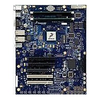
Manufacturer Part Number
MPC8572DS
Description
KIT MPU POWERQUICC III
Manufacturer
Freescale Semiconductor
Series
PowerQUICC III™r
Type
MPUr
Specifications of MPC8572DS
Contents
Board
Data Rate
10 Mbps to 100 Mbps
Memory Type
Flash, DDR, DDR2, DDR3, SDRAM
Interface Type
I2C, Ethernet
Operating Voltage
3.3 V
Data Bus Width
32 bit
Product
Development Tools
Silicon Manufacturer
Freescale
Core Architecture
Power Architecture
Core Sub-architecture
PowerQUICC
Silicon Core Number
MPC85xx
Silicon Family Name
PowerQUICC III
Rohs Compliant
Yes
For Use With/related Products
MPC8572E
Lead Free Status / RoHS Status
Lead free / RoHS Compliant


High-Speed Serial Interfaces (HSSI)
15.2.3
76
•
•
•
SD n _REF_CLK
SD n _REF_CLK
With on-chip termination to SGND_SRDSn (xcorevss), the differential reference clocks inputs are
HCSL (High-Speed Current Steering Logic) compatible DC-coupled.
Many other low voltage differential type outputs like LVDS (Low Voltage Differential Signaling)
can be used but may need to be AC-coupled due to the limited common mode input range allowed
(100 to 400 mV) for DC-coupled connection.
LVPECL outputs can produce signal with too large amplitude and may need to be DC-biased at
clock driver output first, then followed with series attenuation resistor to reduce the amplitude,
additionally to AC-coupling.
Figure 46. Differential Reference Clock Input DC Requirements (External AC-Coupled)
Interfacing With Other Differential Signaling Levels
SD n _REF_CLK
SD n _REF_CLK
MPC8572E PowerQUICC III Integrated Processor Hardware Specifications, Rev. 5
Figure 47. Single-Ended Reference Clock Input DC Requirements
200 mV < Input Amplitude or Differential Peak < 800 mV
400 mV
<
SD n _REF_CLK Input Amplitude
<
800 mV
Vmin
Vmax
0 V
Freescale Semiconductor
>
<
Vcm – 400 mV
Vcm + 400 mV
Vcm
Related parts for MPC8572DS
Image
Part Number
Description
Manufacturer
Datasheet
Request
R

Part Number:
Description:
Manufacturer:
Freescale Semiconductor, Inc
Datasheet:
Part Number:
Description:
Manufacturer:
Freescale Semiconductor, Inc
Datasheet:
Part Number:
Description:
Manufacturer:
Freescale Semiconductor, Inc
Datasheet:
Part Number:
Description:
Manufacturer:
Freescale Semiconductor, Inc
Datasheet:
Part Number:
Description:
Manufacturer:
Freescale Semiconductor, Inc
Datasheet:
Part Number:
Description:
Manufacturer:
Freescale Semiconductor, Inc
Datasheet:
Part Number:
Description:
Manufacturer:
Freescale Semiconductor, Inc
Datasheet:
Part Number:
Description:
Manufacturer:
Freescale Semiconductor, Inc
Datasheet:
Part Number:
Description:
Manufacturer:
Freescale Semiconductor, Inc
Datasheet:
Part Number:
Description:
Manufacturer:
Freescale Semiconductor, Inc
Datasheet:
Part Number:
Description:
Manufacturer:
Freescale Semiconductor, Inc
Datasheet:
Part Number:
Description:
Manufacturer:
Freescale Semiconductor, Inc
Datasheet:
Part Number:
Description:
Manufacturer:
Freescale Semiconductor, Inc
Datasheet:
Part Number:
Description:
Manufacturer:
Freescale Semiconductor, Inc
Datasheet:
Part Number:
Description:
Manufacturer:
Freescale Semiconductor, Inc
Datasheet: