MPC8572DS Freescale Semiconductor, MPC8572DS Datasheet - Page 59
MPC8572DS
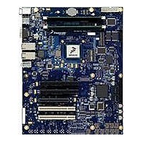
Manufacturer Part Number
MPC8572DS
Description
KIT MPU POWERQUICC III
Manufacturer
Freescale Semiconductor
Series
PowerQUICC III™r
Type
MPUr
Specifications of MPC8572DS
Contents
Board
Data Rate
10 Mbps to 100 Mbps
Memory Type
Flash, DDR, DDR2, DDR3, SDRAM
Interface Type
I2C, Ethernet
Operating Voltage
3.3 V
Data Bus Width
32 bit
Product
Development Tools
Silicon Manufacturer
Freescale
Core Architecture
Power Architecture
Core Sub-architecture
PowerQUICC
Silicon Core Number
MPC85xx
Silicon Family Name
PowerQUICC III
Rohs Compliant
Yes
For Use With/related Products
MPC8572E
Lead Free Status / RoHS Status
Lead free / RoHS Compliant


At recommended operating conditions with BV
Freescale Semiconductor
LALE output negation to high impedance for
LAD/LDP (LATCH hold time)
Local bus clock to output valid (except LAD/LDP and
LALE)
Local bus clock to data valid for LAD/LDP
Local bus clock to address valid for LAD
Local bus clock to LALE assertion
Output hold from local bus clock (except LAD/LDP
and LALE)
Output hold from local bus clock for LAD/LDP
Local bus clock to output high Impedance (except
LAD/LDP and LALE)
Local bus clock to output high impedance for
LAD/LDP
Notes:
1. The symbols used for timing specifications herein follow the pattern of t
2. All timings are in reference to local bus clock for PLL bypass mode. Timings may be negative with respect to the local bus
3. Maximum possible clock skew between a clock LCLK[m] and a relative clock LCLK[n]. Skew measured between
4. All signals are measured from BVDD/2 of the rising edge of local bus clock for PLL bypass mode to 0.4 x BVDD of the signal
5. Input timings are measured at the pin.
6. t
7. For purposes of active/float timing measurements, the Hi-Z or off state is defined to be when the total current delivered through
for inputs and t
timing (LB) for the input (I) to go invalid (X) with respect to the time the t
clock one(1). Also, t
output (O) going invalid (X) or output hold time.
clock because the actual launch and capture of signals is done with the internal launch/capture clock, which precedes LCLK
by t
complementary signals at BV
in question for 3.3-V signaling levels.
programmed with the LBCR[AHD] parameter.
the component pin is less than or equal to the leakage current specification.
LBOTOT
LBKHKT
is a measurement of the minimum time between the negation of LALE and any change in LAD. t
.
(First two letters of functional block)(reference)(state)(signal)(state)
Table 52. Local Bus General Timing Parameters—PLL Bypassed (continued)
In PLL bypass mode, LCLK[n] is the inverted version of the internal clock
with the delay of
of the internal clock and are captured at the falling edge of the internal clock
with the exception of LGTA/LUPWAIT (which is captured on the rising
edge of the internal clock).
MPC8572E PowerQUICC III Integrated Processor Hardware Specifications, Rev. 5
Parameter
LBKHOX
symbolizes local bus timing (LB) for the t
DD
/2.
t
LBKHKT.
DD
of 3.3 V ± 5%
In this mode, signals are launched at the rising edge
Symbol
t
t
t
t
t
t
t
t
t
LBKLOV1
LBKLOV2
LBKLOV3
LBKLOV4
LBKLOX1
LBKLOX2
LBKLOZ1
LBKLOZ2
LBOTOT
NOTE
1
LBK
for outputs. For example, t
(First two letters of functional block)(signal)(state) (reference)(state)
LBK
clock reference (K) to go high (H), with respect to the
–3.3
–3.3
Min
1.5
—
—
—
—
—
—
clock reference (K) goes high (H), in this case for
Max
–0.3
–0.1
0.0
0.0
0.2
0.2
—
—
—
LBIXKH1
Local Bus Controller (eLBC)
symbolizes local bus
LBOTOT
Unit
ns
ns
ns
ns
ns
ns
ns
ns
ns
is
Notes
6
4
4
4
4
4
7
7
59
Related parts for MPC8572DS
Image
Part Number
Description
Manufacturer
Datasheet
Request
R

Part Number:
Description:
Manufacturer:
Freescale Semiconductor, Inc
Datasheet:
Part Number:
Description:
Manufacturer:
Freescale Semiconductor, Inc
Datasheet:
Part Number:
Description:
Manufacturer:
Freescale Semiconductor, Inc
Datasheet:
Part Number:
Description:
Manufacturer:
Freescale Semiconductor, Inc
Datasheet:
Part Number:
Description:
Manufacturer:
Freescale Semiconductor, Inc
Datasheet:
Part Number:
Description:
Manufacturer:
Freescale Semiconductor, Inc
Datasheet:
Part Number:
Description:
Manufacturer:
Freescale Semiconductor, Inc
Datasheet:
Part Number:
Description:
Manufacturer:
Freescale Semiconductor, Inc
Datasheet:
Part Number:
Description:
Manufacturer:
Freescale Semiconductor, Inc
Datasheet:
Part Number:
Description:
Manufacturer:
Freescale Semiconductor, Inc
Datasheet:
Part Number:
Description:
Manufacturer:
Freescale Semiconductor, Inc
Datasheet:
Part Number:
Description:
Manufacturer:
Freescale Semiconductor, Inc
Datasheet:
Part Number:
Description:
Manufacturer:
Freescale Semiconductor, Inc
Datasheet:
Part Number:
Description:
Manufacturer:
Freescale Semiconductor, Inc
Datasheet:
Part Number:
Description:
Manufacturer:
Freescale Semiconductor, Inc
Datasheet: