MPC8572DS Freescale Semiconductor, MPC8572DS Datasheet - Page 19
MPC8572DS
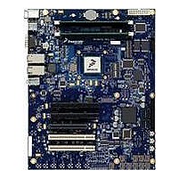
Manufacturer Part Number
MPC8572DS
Description
KIT MPU POWERQUICC III
Manufacturer
Freescale Semiconductor
Series
PowerQUICC III™r
Type
MPUr
Specifications of MPC8572DS
Contents
Board
Data Rate
10 Mbps to 100 Mbps
Memory Type
Flash, DDR, DDR2, DDR3, SDRAM
Interface Type
I2C, Ethernet
Operating Voltage
3.3 V
Data Bus Width
32 bit
Product
Development Tools
Silicon Manufacturer
Freescale
Core Architecture
Power Architecture
Core Sub-architecture
PowerQUICC
Silicon Core Number
MPC85xx
Silicon Family Name
PowerQUICC III
Rohs Compliant
Yes
For Use With/related Products
MPC8572E
Lead Free Status / RoHS Status
Lead free / RoHS Compliant


Table 10
6
This section describes the DC and AC electrical specifications for the DDR2 and DDR3 SDRAM
controller interface of the MPC8572E. Note that the required GV
interfacing to DDR2 or DDR3 SDRAM, respectively.
6.1
Table 11
MPC8572E when interfacing to DDR2 SDRAM.
Freescale Semiconductor
I/O supply voltage
I/O reference voltage
I/O termination voltage
Input high voltage
Input low voltage
Output leakage current
Output high current (V
Output low current (V
Notes:
1. GV
2. MV
3. V
4. Output leakage is measured with all outputs disabled, 0 V
Peak-to-peak noise on MV
equal to MV
PLL lock times
Local bus PLL
TT
DD
REF
DDR2 and DDR3 SDRAM Controller
is not applied directly to the device. It is the supply to that far end signal termination is made and is expected to be
provides the recommended operating conditions for the DDR SDRAM controller of the
provides the PLL lock times.
is expected to be within 50 mV of the DRAM GV
DDR2 and DDR3 SDRAM Interface DC Electrical Characteristics
n is expected to be equal to 0.5 × GV
Parameter/Condition
Table 11. DDR2 SDRAM Interface DC Electrical Characteristics for GV
REF
MPC8572E PowerQUICC III Integrated Processor Hardware Specifications, Rev. 5
n . This rail should track variations in the DC level of MV
Parameter/Condition
OUT
OUT
= 0.280 V)
= 1.420 V)
REF
n may not exceed ±2% of the DC value.
Table 10. PLL Lock Times
DD
Symbol
MV
GV
, and to track GV
V
V
V
I
I
I
OZ
OH
OL
REF
TT
IH
IL
DD
n
DD
MV
at all times.
Symbol
≤
MV
0.49 × GV
V
—
—
REF
REF
OUT
–13.4
DD
1.71
–0.3
13.4
Min
–50
n + 0.125
n – 0.04
≤
DC variations as measured at the receiver.
GV
DD
REF
DD
DD
.
n .
Min
100
50
(typ) voltage is 1.8Vor 1.5 V when
MV
MV
0.51 × GV
GV
REF
REF
DD
Max
1.89
n – 0.125
50
—
—
n + 0.04
+ 0.3
DDR2 and DDR3 SDRAM Controller
DD
DD
Typical
(typ) = 1.8 V
μs
μs
Unit
mA
mA
μA
V
V
V
V
V
Max
—
—
Notes
—
—
—
—
1
2
3
4
19
Related parts for MPC8572DS
Image
Part Number
Description
Manufacturer
Datasheet
Request
R

Part Number:
Description:
Manufacturer:
Freescale Semiconductor, Inc
Datasheet:
Part Number:
Description:
Manufacturer:
Freescale Semiconductor, Inc
Datasheet:
Part Number:
Description:
Manufacturer:
Freescale Semiconductor, Inc
Datasheet:
Part Number:
Description:
Manufacturer:
Freescale Semiconductor, Inc
Datasheet:
Part Number:
Description:
Manufacturer:
Freescale Semiconductor, Inc
Datasheet:
Part Number:
Description:
Manufacturer:
Freescale Semiconductor, Inc
Datasheet:
Part Number:
Description:
Manufacturer:
Freescale Semiconductor, Inc
Datasheet:
Part Number:
Description:
Manufacturer:
Freescale Semiconductor, Inc
Datasheet:
Part Number:
Description:
Manufacturer:
Freescale Semiconductor, Inc
Datasheet:
Part Number:
Description:
Manufacturer:
Freescale Semiconductor, Inc
Datasheet:
Part Number:
Description:
Manufacturer:
Freescale Semiconductor, Inc
Datasheet:
Part Number:
Description:
Manufacturer:
Freescale Semiconductor, Inc
Datasheet:
Part Number:
Description:
Manufacturer:
Freescale Semiconductor, Inc
Datasheet:
Part Number:
Description:
Manufacturer:
Freescale Semiconductor, Inc
Datasheet:
Part Number:
Description:
Manufacturer:
Freescale Semiconductor, Inc
Datasheet: