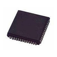
MC68HC11E1CFN3 Freescale Semiconductor, MC68HC11E1CFN3 Datasheet - Page 24

MC68HC11E1CFN3
Manufacturer Part Number
MC68HC11E1CFN3
Description
IC MCU 3MHZ 512 EEPROM 52-PLCC
Manufacturer
Freescale Semiconductor
Series
HC11r
Datasheet
1.MC68HC11E1CFN3.pdf
(268 pages)
Specifications of MC68HC11E1CFN3
Core Processor
HC11
Core Size
8-Bit
Speed
3MHz
Connectivity
SCI, SPI
Peripherals
POR, WDT
Number Of I /o
38
Program Memory Type
ROMless
Eeprom Size
512 x 8
Ram Size
512 x 8
Voltage - Supply (vcc/vdd)
4.5 V ~ 5.5 V
Data Converters
A/D 8x8b
Oscillator Type
Internal
Operating Temperature
-40°C ~ 85°C
Package / Case
52-PLCC
Data Bus Width
8 bit
Data Ram Size
512 B
Interface Type
SCI, SPI
Maximum Clock Frequency
3 MHz
Number Of Programmable I/os
22
Number Of Timers
16 bit
Maximum Operating Temperature
+ 85 C
Mounting Style
SMD/SMT
Minimum Operating Temperature
- 40 C
On-chip Adc
8 bit
Lead Free Status / RoHS Status
Contains lead / RoHS non-compliant
Program Memory Size
-
Lead Free Status / Rohs Status
Details
Available stocks
Company
Part Number
Manufacturer
Quantity
Price
Company:
Part Number:
MC68HC11E1CFN3
Manufacturer:
MOT
Quantity:
2 600
Company:
Part Number:
MC68HC11E1CFN3
Manufacturer:
MOTOROLA
Quantity:
2 337
Company:
Part Number:
MC68HC11E1CFN3
Manufacturer:
Freescale Semiconductor
Quantity:
10 000
Part Number:
MC68HC11E1CFN3
Manufacturer:
MOTOROLA/摩托罗拉
Quantity:
20 000
- Current page: 24 of 268
- Download datasheet (4Mb)
General Description
1.4.2 RESET
1.4.3 Crystal Driver and External Clock Input (XTAL and EXTAL)
Data Sheet
24
CAUTION:
A bidirectional control signal, RESET, acts as an input to initialize the MCU to a
known startup state. It also acts as an open-drain output to indicate that an internal
failure has been detected in either the clock monitor or computer operating properly
(COP) watchdog circuit. The CPU distinguishes between internal and external
reset conditions by sensing whether the reset pin rises to a logic 1 in less than two
E-clock cycles after a reset has occurred. See
Do not connect an external resistor capacitor (RC) power-up delay circuit to the
reset pin of M68HC11 devices because the circuit charge time constant can cause
the device to misinterpret the type of reset that occurred.
Because the CPU is not able to fetch and execute instructions properly when V
falls below the minimum operating voltage level, reset must be controlled. A
low-voltage inhibit (LVI) circuit is required primarily for protection of EEPROM
contents. However, since the configuration register (CONFIG) value is read from
the EEPROM, protection is required even if the EEPROM array is not being used.
Presently, there are several economical ways to solve this problem. For example,
two good external components for LVI reset are:
Refer to
These two pins provide the interface for either a crystal or a CMOS- compatible
clock to control the internal clock generator circuitry. The frequency applied to
these pins is four times higher than the desired E-clock rate.
The XTAL pin must be left unterminated when an external CMOS- compatible clock
input is connected to the EXTAL pin. The XTAL output is normally intended to drive
only a crystal. Refer to
1. The Seiko S0854HN (or other S805 series devices):
2. The Motorola MC34064:
Freescale Semiconductor, Inc.
a. Extremely low power (2 µA)
a. TO-92 package
a. Limited temperature range, –20°C to +70°C
a. Available in various trip-point voltage ranges
a. TO-92 or SO-8 package
a. Draws about 300 µA
a. Temperature range –40°C to 85°C
a. Well controlled trip point
a. Inexpensive
Section 5. Resets and Interrupts
For More Information On This Product,
Go to: www.freescale.com
General Description
Figure 1-9
and
Figure
for further information.
1-10.
Figure 1-7
M68HC11E Family — Rev. 5
and
Figure
1-8.
MOTOROLA
DD
Related parts for MC68HC11E1CFN3
Image
Part Number
Description
Manufacturer
Datasheet
Request
R

Part Number:
Description:
MC68HC11 EEPROM Programming from a Personal Computer
Manufacturer:
Motorola / Freescale Semiconductor
Part Number:
Description:
Manufacturer:
Freescale Semiconductor, Inc
Datasheet:
Part Number:
Description:
Manufacturer:
Freescale Semiconductor, Inc
Datasheet:
Part Number:
Description:
Manufacturer:
Freescale Semiconductor, Inc
Datasheet:
Part Number:
Description:
Manufacturer:
Freescale Semiconductor, Inc
Datasheet:
Part Number:
Description:
Manufacturer:
Freescale Semiconductor, Inc
Datasheet:
Part Number:
Description:
Manufacturer:
Freescale Semiconductor, Inc
Datasheet:
Part Number:
Description:
Manufacturer:
Freescale Semiconductor, Inc
Datasheet:
Part Number:
Description:
Manufacturer:
Freescale Semiconductor, Inc
Datasheet:
Part Number:
Description:
Manufacturer:
Freescale Semiconductor, Inc
Datasheet:
Part Number:
Description:
Manufacturer:
Freescale Semiconductor, Inc
Datasheet:
Part Number:
Description:
Manufacturer:
Freescale Semiconductor, Inc
Datasheet:
Part Number:
Description:
Manufacturer:
Freescale Semiconductor, Inc
Datasheet:
Part Number:
Description:
Manufacturer:
Freescale Semiconductor, Inc
Datasheet:
Part Number:
Description:
Manufacturer:
Freescale Semiconductor, Inc
Datasheet:


