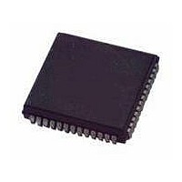
MC68HC11E1CFN3 Freescale Semiconductor, MC68HC11E1CFN3 Datasheet - Page 42

MC68HC11E1CFN3
Manufacturer Part Number
MC68HC11E1CFN3
Description
IC MCU 3MHZ 512 EEPROM 52-PLCC
Manufacturer
Freescale Semiconductor
Series
HC11r
Datasheet
1.MC68HC11E1CFN3.pdf
(268 pages)
Specifications of MC68HC11E1CFN3
Core Processor
HC11
Core Size
8-Bit
Speed
3MHz
Connectivity
SCI, SPI
Peripherals
POR, WDT
Number Of I /o
38
Program Memory Type
ROMless
Eeprom Size
512 x 8
Ram Size
512 x 8
Voltage - Supply (vcc/vdd)
4.5 V ~ 5.5 V
Data Converters
A/D 8x8b
Oscillator Type
Internal
Operating Temperature
-40°C ~ 85°C
Package / Case
52-PLCC
Data Bus Width
8 bit
Data Ram Size
512 B
Interface Type
SCI, SPI
Maximum Clock Frequency
3 MHz
Number Of Programmable I/os
22
Number Of Timers
16 bit
Maximum Operating Temperature
+ 85 C
Mounting Style
SMD/SMT
Minimum Operating Temperature
- 40 C
On-chip Adc
8 bit
Lead Free Status / RoHS Status
Contains lead / RoHS non-compliant
Program Memory Size
-
Lead Free Status / Rohs Status
Details
Available stocks
Company
Part Number
Manufacturer
Quantity
Price
Company:
Part Number:
MC68HC11E1CFN3
Manufacturer:
MOT
Quantity:
2 600
Company:
Part Number:
MC68HC11E1CFN3
Manufacturer:
MOTOROLA
Quantity:
2 337
Company:
Part Number:
MC68HC11E1CFN3
Manufacturer:
Freescale Semiconductor
Quantity:
10 000
Part Number:
MC68HC11E1CFN3
Manufacturer:
MOTOROLA/摩托罗拉
Quantity:
20 000
- Current page: 42 of 268
- Download datasheet (4Mb)
Operating Modes and On-Chip Memory
Data Sheet
42
1. SCP2 adds ÷39 to SCI prescaler and is present only in MC68HC(7)11E20.
$102A
$102B
$102C
$102D
$102E
$102F
$1030
$1031
$1032
$1033
$1034
$1035
Addr.
Analog-to-Digital Control Status
Serial Communications Control
Serial Communications Control
Serial Communications Status
Serial Communications Data
Serial Peripheral Data I/O
Analog-to-Digital Results
Analog-to-Digital Results
Analog-to-Digital Results
Analog-to-Digital Results
Register Name
Block Protect Register
Register 1 (SCCR1)
Register 2 (SCCR2)
Baud Rate Register
Register 1 (ADR1)
Register 2 (ADR2)
Register 3 (ADR3)
Register 4 (ADR4)
Register (ADCTL)
Figure 2-7. Register and Control Bit Assignments (Sheet 5 of 6)
Register (SCDR)
Register (SPDR)
Register (SCSR)
See page 140.
See page 126.
See page 123.
See page 124.
See page 125.
See page 122.
See page 69.
See page 71.
See page 71.
See page 71.
See page 71.
See page 58.
(BPROT)
(BAUD)
Freescale Semiconductor, Inc.
For More Information On This Product,
Reset:
Reset:
Reset:
Reset:
Reset:
Reset:
Reset:
Reset:
Reset:
Reset:
Reset:
Reset:
Read:
Read:
Read:
Read:
Read:
Read:
Read:
Read:
Read:
Read:
Read:
Read:
Write:
Write:
Write:
Write:
Write:
Write:
Write:
Write:
Write:
Write:
Write:
Write:
Operating Modes and On-Chip Memory
I = Indeterminate after reset
TCLR
TDRE
R7/T7
CCF
Bit 7
Bit 7
Bit 7
Bit 7
Bit 7
Bit 7
TIE
R8
Go to: www.freescale.com
0
0
1
0
0
I
= Unimplemented
SCP2
R6/T6
Bit 6
Bit 6
Bit 6
Bit 6
TCIE
Bit 6
TC
T8
6
0
0
1
0
0
I
(1)
RDRF
R5/T5
SCAN
SCP1
Bit 5
Bit 5
Bit 5
Bit 5
Bit 5
RIE
5
0
0
0
0
0
Indeterminate after reset
Indeterminate after reset
Indeterminate after reset
Indeterminate after reset
Indeterminate after reset
Indeterminate after reset
PTCON
MULT
SCP0
R4/T4
Bit 4
Bit 4
Bit 4
Bit 4
IDLE
Bit 4
ILIE
M
R
0
0
0
0
1
4
Indeterminate after reset
= Reserved
BPRT3
WAKE
RCKB
R3/T3
Bit 3
Bit 3
Bit 3
Bit 3
Bit 3
OR
CD
TE
3
0
0
0
0
1
M68HC11E Family — Rev. 5
BPRT2
SCR2
R2/T2
U = Unaffected
Bit 2
Bit 2
Bit 2
Bit 2
Bit 2
RE
NF
CC
U
2
0
0
0
1
BPRT1
SCR1
R1/T1
RWU
Bit 1
Bit 1
Bit 1
Bit 1
Bit 1
CB
FE
U
1
0
0
0
1
MOTOROLA
BPRT0
R0/T0
SCR0
Bit 0
Bit 0
Bit 0
Bit 0
Bit 0
Bit 0
SBK
CA
U
0
0
0
1
Related parts for MC68HC11E1CFN3
Image
Part Number
Description
Manufacturer
Datasheet
Request
R

Part Number:
Description:
MC68HC11 EEPROM Programming from a Personal Computer
Manufacturer:
Motorola / Freescale Semiconductor
Part Number:
Description:
Manufacturer:
Freescale Semiconductor, Inc
Datasheet:
Part Number:
Description:
Manufacturer:
Freescale Semiconductor, Inc
Datasheet:
Part Number:
Description:
Manufacturer:
Freescale Semiconductor, Inc
Datasheet:
Part Number:
Description:
Manufacturer:
Freescale Semiconductor, Inc
Datasheet:
Part Number:
Description:
Manufacturer:
Freescale Semiconductor, Inc
Datasheet:
Part Number:
Description:
Manufacturer:
Freescale Semiconductor, Inc
Datasheet:
Part Number:
Description:
Manufacturer:
Freescale Semiconductor, Inc
Datasheet:
Part Number:
Description:
Manufacturer:
Freescale Semiconductor, Inc
Datasheet:
Part Number:
Description:
Manufacturer:
Freescale Semiconductor, Inc
Datasheet:
Part Number:
Description:
Manufacturer:
Freescale Semiconductor, Inc
Datasheet:
Part Number:
Description:
Manufacturer:
Freescale Semiconductor, Inc
Datasheet:
Part Number:
Description:
Manufacturer:
Freescale Semiconductor, Inc
Datasheet:
Part Number:
Description:
Manufacturer:
Freescale Semiconductor, Inc
Datasheet:
Part Number:
Description:
Manufacturer:
Freescale Semiconductor, Inc
Datasheet:


