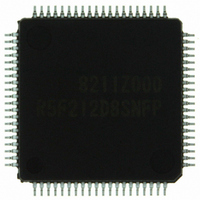
R5F212D8SNFP#U0 Renesas Electronics America, R5F212D8SNFP#U0 Datasheet - Page 263

R5F212D8SNFP#U0
Manufacturer Part Number
R5F212D8SNFP#U0
Description
IC R8C/2D MCU FLASH 64KB 80-LQFP
Manufacturer
Renesas Electronics America
Series
R8C/2x/2Dr
Specifications of R5F212D8SNFP#U0
Core Processor
R8C
Core Size
16/32-Bit
Speed
20MHz
Connectivity
I²C, LIN, SIO, SSU, UART/USART
Peripherals
POR, PWM, Voltage Detect, WDT
Number Of I /o
71
Program Memory Size
64KB (64K x 8)
Program Memory Type
FLASH
Ram Size
3K x 8
Voltage - Supply (vcc/vdd)
2.2 V ~ 5.5 V
Data Converters
A/D 20x10b; D/A 2x8b
Oscillator Type
Internal
Operating Temperature
-20°C ~ 85°C
Package / Case
80-LQFP
For Use With
R0K5212D8S001BE - KIT STARTER FOR R8C/2DR0K5212D8S000BE - KIT DEV FOR R8C/2D
Lead Free Status / RoHS Status
Lead free / RoHS Compliant
Eeprom Size
-
Available stocks
Company
Part Number
Manufacturer
Quantity
Price
- Current page: 263 of 617
- Download datasheet (7Mb)
R8C/2C Group, R8C/2D Group
Rev.2.00
REJ09B0339-0200
14.4
Table 14.26
The count source is f1, f2, f4, f8, f32, or TRDCLK input
(bits TCK2 to TCK0 in registers TRDCR0 and TRDCR1 are set to a value from 000b
to 101b).
The count source is fOCO40M
(bits TCK2 to TCK0 in registers TRDCR0 and TRDCR1 are set to 110b).
Timer RD has 2 16-bit timers (channels 0 and 1). Each channel has 4 I/O pins.
The operation clock of timer RD is f1 or fOCO40M. Table 14.26 lists the Timer RD Operation Clocks.
Figure 14.62 shows a Block Diagram of Timer RD. Timer RD has 5 modes:
The following 4 modes use the output compare function.
In the input capture function, output compare function, and PWM mode, channels 0 and 1 have the equivalent
functions, and functions or modes can be selected individually for each pin. Also, a combination of these functions
and modes can be used in 1 channel.
In reset synchronous PWM mode, complementary PWM mode, and PWM3 mode, a waveform is output with a
combination of counters and registers in channels 0 and 1.
Tables 14.27 to 14.35 list the Pin Functions of timer RD.
• Timer mode
• PWM mode
• Reset synchronous PWM mode
• Complementary PWM mode
• PWM3 mode
- Input capture function
- Output compare function
Timer RD
Dec 05, 2007
Timer RD Operation Clocks
Page 240 of 585
Condition
Transfer the counter value to a register with an external signal as the
trigger
Detect register value matches with a counter
(Pin output can be changed at detection)
Output pulse of any width continuously
Output three-phase waveforms (6) without sawtooth wave modulation
and dead time
Output three-phase waveforms (6) with triangular wave modulation and
dead time
Output PWM waveforms (2) with a fixed period
f1
fOCO40M
Operation Clock of Timer RD
14. Timers
Related parts for R5F212D8SNFP#U0
Image
Part Number
Description
Manufacturer
Datasheet
Request
R

Part Number:
Description:
KIT STARTER FOR M16C/29
Manufacturer:
Renesas Electronics America
Datasheet:

Part Number:
Description:
KIT STARTER FOR R8C/2D
Manufacturer:
Renesas Electronics America
Datasheet:

Part Number:
Description:
R0K33062P STARTER KIT
Manufacturer:
Renesas Electronics America
Datasheet:

Part Number:
Description:
KIT STARTER FOR R8C/23 E8A
Manufacturer:
Renesas Electronics America
Datasheet:

Part Number:
Description:
KIT STARTER FOR R8C/25
Manufacturer:
Renesas Electronics America
Datasheet:

Part Number:
Description:
KIT STARTER H8S2456 SHARPE DSPLY
Manufacturer:
Renesas Electronics America
Datasheet:

Part Number:
Description:
KIT STARTER FOR R8C38C
Manufacturer:
Renesas Electronics America
Datasheet:

Part Number:
Description:
KIT STARTER FOR R8C35C
Manufacturer:
Renesas Electronics America
Datasheet:

Part Number:
Description:
KIT STARTER FOR R8CL3AC+LCD APPS
Manufacturer:
Renesas Electronics America
Datasheet:

Part Number:
Description:
KIT STARTER FOR RX610
Manufacturer:
Renesas Electronics America
Datasheet:

Part Number:
Description:
KIT STARTER FOR R32C/118
Manufacturer:
Renesas Electronics America
Datasheet:

Part Number:
Description:
KIT DEV RSK-R8C/26-29
Manufacturer:
Renesas Electronics America
Datasheet:

Part Number:
Description:
KIT STARTER FOR SH7124
Manufacturer:
Renesas Electronics America
Datasheet:

Part Number:
Description:
KIT STARTER FOR H8SX/1622
Manufacturer:
Renesas Electronics America
Datasheet:

Part Number:
Description:
KIT DEV FOR SH7203
Manufacturer:
Renesas Electronics America
Datasheet:


