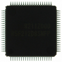
R5F212D8SNFP#U0 Renesas Electronics America, R5F212D8SNFP#U0 Datasheet - Page 613

R5F212D8SNFP#U0
Manufacturer Part Number
R5F212D8SNFP#U0
Description
IC R8C/2D MCU FLASH 64KB 80-LQFP
Manufacturer
Renesas Electronics America
Series
R8C/2x/2Dr
Specifications of R5F212D8SNFP#U0
Core Processor
R8C
Core Size
16/32-Bit
Speed
20MHz
Connectivity
I²C, LIN, SIO, SSU, UART/USART
Peripherals
POR, PWM, Voltage Detect, WDT
Number Of I /o
71
Program Memory Size
64KB (64K x 8)
Program Memory Type
FLASH
Ram Size
3K x 8
Voltage - Supply (vcc/vdd)
2.2 V ~ 5.5 V
Data Converters
A/D 20x10b; D/A 2x8b
Oscillator Type
Internal
Operating Temperature
-20°C ~ 85°C
Package / Case
80-LQFP
For Use With
R0K5212D8S001BE - KIT STARTER FOR R8C/2DR0K5212D8S000BE - KIT DEV FOR R8C/2D
Lead Free Status / RoHS Status
Lead free / RoHS Compliant
Eeprom Size
-
Available stocks
Company
Part Number
Manufacturer
Quantity
Price
- Current page: 613 of 617
- Download datasheet (7Mb)
Rev.
2.00
REVISION HISTORY
Dec 05, 2007
Date
34, 155,
Page
499
102
103
107
120
139
150
159
160
161
165
176
177
180
183
20
23
34
31
35
36
74
78
85
86
97
Table 4.1 002Ch: High-Speed On-Chip Oscillator Control Register 7
Figure 10.6 FRA1 revised
Figure 10.7 FRA2: NOTE2 deleted, FRA7 added
10.2.2 “The frequency correction .... to the FRA1 before use.” added
10.6.1 “To use the high-speed on-chip oscillator clock for the CPU clock
12.2.1 “.... with the pulse output forced cutoff of timer RD and the INT1
Table 14.1 Timer RE: Count sources “• fC32” deleted
Table 14.2 Timer RC: “TRDIOA” → “TRCIOA”, “TRDIOB” → “TRCIOB”,
14.1.6 “• When the TRAPRE register is .... for each write interval.
14.2 “The reload register and counter are allocated at the same
Figure 14.15 “Programmable one-shot mode” → “Programmable one-
Figure 14.17 “Both bits TSTART .... are set to 0 (During count).”
Table 4.4 00F5h: After reset “00h” → “000000XXb” revised
Figure 5.3 revised
Figure 5.4, Figure 13.3, Figure 20.4 OFS NOTE1 revised
Table 5.1 Rated Value: “TBD” → “700”
5.1.1, 5.1.2 “Wait for 1/fOCO-S × 20.” → “Wait for 10 µ s or more.”
Figure 5.5, Figure 5.6 revised
Table 7.17 Function: RXD0 input NOTE1 added
Table 7.29 revised
Table 7.57 Function: Input port NOTE1 added
Table 7.58 Function: RXD2 input NOTE1 added
Table 7.61 Function: RXD1 input NOTE1 added
Figure 10.1 “Clock prescaler” added
Figure 12.22 NOTE2 revised
Figure 14.1 “TSTART” → “TCSTF”
Figure 14.5 “Both bits TSTART ... are set to 0 (During count).”
R8C/2C Group, R8C/2D Group Hardware Manual
address” deleted
• When the TRA register is .... for each write interval.” added
.... and then set bits OCD1 to OCD0 to 11b.” revised
pin is shared with the external trigger input pin of timer RA.”
→ “.... with the pulse output forced cutoff of timer RC and timer
RD, and the external trigger input of timer RB.”
added
Timer RF: Input pin “TCIN” → “TRFI”
→ “Both bits TSTART ... are set to 1 (During count).”
shot generation mode”
→ “Both bits TSTART .... are set to 1 (During count).”
C - 5
“TRDIOC” → “TRCIOC”, “TRDIOD” → “TRCIOD”
Description
Summary
Related parts for R5F212D8SNFP#U0
Image
Part Number
Description
Manufacturer
Datasheet
Request
R

Part Number:
Description:
KIT STARTER FOR M16C/29
Manufacturer:
Renesas Electronics America
Datasheet:

Part Number:
Description:
KIT STARTER FOR R8C/2D
Manufacturer:
Renesas Electronics America
Datasheet:

Part Number:
Description:
R0K33062P STARTER KIT
Manufacturer:
Renesas Electronics America
Datasheet:

Part Number:
Description:
KIT STARTER FOR R8C/23 E8A
Manufacturer:
Renesas Electronics America
Datasheet:

Part Number:
Description:
KIT STARTER FOR R8C/25
Manufacturer:
Renesas Electronics America
Datasheet:

Part Number:
Description:
KIT STARTER H8S2456 SHARPE DSPLY
Manufacturer:
Renesas Electronics America
Datasheet:

Part Number:
Description:
KIT STARTER FOR R8C38C
Manufacturer:
Renesas Electronics America
Datasheet:

Part Number:
Description:
KIT STARTER FOR R8C35C
Manufacturer:
Renesas Electronics America
Datasheet:

Part Number:
Description:
KIT STARTER FOR R8CL3AC+LCD APPS
Manufacturer:
Renesas Electronics America
Datasheet:

Part Number:
Description:
KIT STARTER FOR RX610
Manufacturer:
Renesas Electronics America
Datasheet:

Part Number:
Description:
KIT STARTER FOR R32C/118
Manufacturer:
Renesas Electronics America
Datasheet:

Part Number:
Description:
KIT DEV RSK-R8C/26-29
Manufacturer:
Renesas Electronics America
Datasheet:

Part Number:
Description:
KIT STARTER FOR SH7124
Manufacturer:
Renesas Electronics America
Datasheet:

Part Number:
Description:
KIT STARTER FOR H8SX/1622
Manufacturer:
Renesas Electronics America
Datasheet:

Part Number:
Description:
KIT DEV FOR SH7203
Manufacturer:
Renesas Electronics America
Datasheet:


