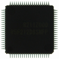
R5F212D8SNFP#U0 Renesas Electronics America, R5F212D8SNFP#U0 Datasheet - Page 57

R5F212D8SNFP#U0
Manufacturer Part Number
R5F212D8SNFP#U0
Description
IC R8C/2D MCU FLASH 64KB 80-LQFP
Manufacturer
Renesas Electronics America
Series
R8C/2x/2Dr
Specifications of R5F212D8SNFP#U0
Core Processor
R8C
Core Size
16/32-Bit
Speed
20MHz
Connectivity
I²C, LIN, SIO, SSU, UART/USART
Peripherals
POR, PWM, Voltage Detect, WDT
Number Of I /o
71
Program Memory Size
64KB (64K x 8)
Program Memory Type
FLASH
Ram Size
3K x 8
Voltage - Supply (vcc/vdd)
2.2 V ~ 5.5 V
Data Converters
A/D 20x10b; D/A 2x8b
Oscillator Type
Internal
Operating Temperature
-20°C ~ 85°C
Package / Case
80-LQFP
For Use With
R0K5212D8S001BE - KIT STARTER FOR R8C/2DR0K5212D8S000BE - KIT DEV FOR R8C/2D
Lead Free Status / RoHS Status
Lead free / RoHS Compliant
Eeprom Size
-
Available stocks
Company
Part Number
Manufacturer
Quantity
Price
- Current page: 57 of 617
- Download datasheet (7Mb)
R8C/2C Group, R8C/2D Group
Rev.2.00
REJ09B0339-0200
Figure 5.3
Figure 5.4
Internal reset
signal
Address
(internal address
signal)
CPU clock
Option Function Select Register
RESET pin
b7 b6 b5 b4 b3 b2 b1 b0
NOTES:
fOCO-S
NOTES:
1.
2.
3. If the block including the OFS register is erased, FFh is set to the OFS register.
1
1. Hardware reset.
2. When the “L” input width to the RESET pin is set to fOCO-S clock × 32 cycles or more, setting the RESET pin to “H” also sets the internal
The OFS register is on the flash memory. Write to the OFS register w ith a program. After w riting is completed, do not
w rite additions to the OFS register.
To use the pow er-on reset, set the LVD0ON bit to 0 (voltage monitor 0 reset enabled after hardw are reset).
Dec 05, 2007
reset signal to “H” at the same.
1
Reset Sequence
OFS Register
1
10 cycles or more are needed
fOCO-S clock × 32 cycles
Bit Symbol
CSPROINI
ROMCP1
LVD0ON
WDTON
ROMCR
Symbol
OFS
(b1)
(b4)
(b6)
Page 34 of 585
—
—
—
Start time of flash memory
(CPU clock × 14 cycles)
Watchdog timer start
select bit
Reserved bit
ROM code protect
disabled bit
ROM code protect bit
Reserved bit
Voltage detection 0
circuit start bit
Reserved bit
Count source protect
mode after reset select
bit
(1)
(1)
(2)
Address
Bit Name
0FFFFh
(2)
CPU clock × 28 cycles
0 : Starts w atchdog timer automatically after reset
1 : Watchdog timer is inactive after reset
Set to 1.
0 : ROM code protect disabled
1 : ROMCP1 enabled
0 : ROM code protect enabled
1 : ROM code protect disabled
Set to 1.
0 : Voltage monitor 0 reset enabled after hardw are
1 : Voltage monitor 0 reset disabled after hardw are
Set to 1.
0 : Count source protect mode enabled after reset
1 : Count source protect mode disabled after reset
reset
reset
0FFFCh
0FFFDh
When Shipping
Function
FFh
(3)
0FFFEh
Content of reset vector
5. Resets
RW
RW
RW
RW
RW
RW
RW
RW
RW
Related parts for R5F212D8SNFP#U0
Image
Part Number
Description
Manufacturer
Datasheet
Request
R

Part Number:
Description:
KIT STARTER FOR M16C/29
Manufacturer:
Renesas Electronics America
Datasheet:

Part Number:
Description:
KIT STARTER FOR R8C/2D
Manufacturer:
Renesas Electronics America
Datasheet:

Part Number:
Description:
R0K33062P STARTER KIT
Manufacturer:
Renesas Electronics America
Datasheet:

Part Number:
Description:
KIT STARTER FOR R8C/23 E8A
Manufacturer:
Renesas Electronics America
Datasheet:

Part Number:
Description:
KIT STARTER FOR R8C/25
Manufacturer:
Renesas Electronics America
Datasheet:

Part Number:
Description:
KIT STARTER H8S2456 SHARPE DSPLY
Manufacturer:
Renesas Electronics America
Datasheet:

Part Number:
Description:
KIT STARTER FOR R8C38C
Manufacturer:
Renesas Electronics America
Datasheet:

Part Number:
Description:
KIT STARTER FOR R8C35C
Manufacturer:
Renesas Electronics America
Datasheet:

Part Number:
Description:
KIT STARTER FOR R8CL3AC+LCD APPS
Manufacturer:
Renesas Electronics America
Datasheet:

Part Number:
Description:
KIT STARTER FOR RX610
Manufacturer:
Renesas Electronics America
Datasheet:

Part Number:
Description:
KIT STARTER FOR R32C/118
Manufacturer:
Renesas Electronics America
Datasheet:

Part Number:
Description:
KIT DEV RSK-R8C/26-29
Manufacturer:
Renesas Electronics America
Datasheet:

Part Number:
Description:
KIT STARTER FOR SH7124
Manufacturer:
Renesas Electronics America
Datasheet:

Part Number:
Description:
KIT STARTER FOR H8SX/1622
Manufacturer:
Renesas Electronics America
Datasheet:

Part Number:
Description:
KIT DEV FOR SH7203
Manufacturer:
Renesas Electronics America
Datasheet:


