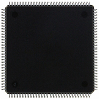
MCF5307AI90B Freescale Semiconductor, MCF5307AI90B Datasheet - Page 116

MCF5307AI90B
Manufacturer Part Number
MCF5307AI90B
Description
IC MPU 32BIT COLDF 90MHZ 208FQFP
Manufacturer
Freescale Semiconductor
Series
MCF530xr
Datasheets
1.MCF5307AI66B.pdf
(484 pages)
2.MCF5307AI66B.pdf
(16 pages)
3.MCF5307AI66B.pdf
(2 pages)
Specifications of MCF5307AI90B
Core Processor
Coldfire V3
Core Size
32-Bit
Speed
90MHz
Connectivity
EBI/EMI, I²C, UART/USART
Peripherals
DMA, POR, WDT
Number Of I /o
16
Program Memory Type
ROMless
Ram Size
4K x 8
Voltage - Supply (vcc/vdd)
3 V ~ 3.6 V
Oscillator Type
External
Operating Temperature
0°C ~ 70°C
Package / Case
208-FQFP
Maximum Clock Frequency
90 MHz
Maximum Operating Temperature
+ 105 C
Mounting Style
SMD/SMT
Minimum Operating Temperature
0 C
Family Name
MCF5xxx
Device Core
ColdFire
Device Core Size
32b
Frequency (max)
90MHz
Instruction Set Architecture
RISC
Supply Voltage 1 (typ)
3.3V
Operating Temp Range
0C to 70C
Operating Temperature Classification
Commercial
Mounting
Surface Mount
Pin Count
208
Package Type
FQFP
Program Memory Size
8KB
Cpu Speed
90MHz
Embedded Interface Type
I2C, UART
Digital Ic Case Style
FQFP
No. Of Pins
208
Supply Voltage Range
3V To 3.6V
Rohs Compliant
Yes
Lead Free Status / RoHS Status
Lead free / RoHS Compliant
Eeprom Size
-
Program Memory Size
-
Data Converters
-
Lead Free Status / Rohs Status
Lead free / RoHS Compliant
Available stocks
Company
Part Number
Manufacturer
Quantity
Price
Company:
Part Number:
MCF5307AI90B
Manufacturer:
FREESCAL
Quantity:
153
Company:
Part Number:
MCF5307AI90B
Manufacturer:
Freescale Semiconductor
Quantity:
10 000
Part Number:
MCF5307AI90B
Manufacturer:
FREESCALE
Quantity:
20 000
- Current page: 116 of 484
- Download datasheet (6Mb)
Freescale Semiconductor, Inc.
Cache Operation
4.9.5.2 Cache Pushes
Cache pushes occur for line replacement and as required for the execution of the CPUSHL
instruction. To reduce the requested data’s latency in the new line, the modified line being
replaced is temporarily placed in the push buffer while the new line is fetched from
memory. After the bus transfer for the new line completes, the modified cache line is written
back to memory and the push buffer is invalidated.
4.9.5.2.1 Push and Store Buffers
The 16-byte push buffer reduces latency for requested new data on a cache miss by holding
a displaced modified cache line while the new data is read from memory.
If a cache miss displaces a modified line, a miss read reference is immediately generated.
While waiting for the response, the current contents of the cache location load into the push
buffer. When the burst-read bus transaction completes, the cache controller can generate the
appropriate line-write bus transaction to write the push buffer contents into memory.
In imprecise mode, the FIFO store buffer can defer pending writes to maximize
performance. The store buffer can support as many as four entries (16 bytes maximum) for
this purpose.
Data writes destined for the store buffer cannot stall the core. The store buffer effectively
provides a measure of decoupling between the pipeline’s ability to generate writes (one per
cycle maximum) and the external bus’s ability to retire those writes. In imprecise mode,
writes stall only if the store buffer is full and a write operation is on the internal bus. The
internal write cycle is held, stalling the data execution pipeline.
If the store buffer is not used (that is, store buffer disabled or cache-inhibited precise mode),
external bus cycles are generated directly for each pipeline write operation. The instruction
is held in the pipeline until external bus transfer termination is received. Therefore, each
write is stalled for 5 cycles, making the minimum write time equal to 6 cycles when the
store buffer is not used. See Section 2.1.2.2, “Operand Execution Pipeline (OEP).”
The store buffer enable bit, CACR[ESB], controls the enabling of the store buffer. This bit
can be set and cleared by the MOVEC instruction. ESB is zero at reset and all writes are
performed in order (precise mode). ACRn[CM] or CACR[DCM] generates the mode used
when ESB is set. Cacheable write-through and cache-inhibited imprecise modes use the
store buffer.
The store buffer can queue data as much as 4 bytes wide per entry. Each entry matches the
corresponding bus cycle it generates; therefore, a misaligned longword write to a
write-through region creates two entries if the address is to an odd-word boundary. It
creates three entries if it is to an odd-byte boundary—one per bus cycle.
4.9.5.2.2 Push and Store Buffer Bus Operation
As soon as the push or store buffer has valid data, the internal bus controller uses the next
available external bus cycle to generate the appropriate write cycles. In the event that
4-18
MCF5307 User’s Manual
For More Information On This Product,
Go to: www.freescale.com
Related parts for MCF5307AI90B
Image
Part Number
Description
Manufacturer
Datasheet
Request
R
Part Number:
Description:
Manufacturer:
Freescale Semiconductor, Inc
Datasheet:
Part Number:
Description:
Mcf5307 Coldfire Integrated Microprocessor User
Manufacturer:
Freescale Semiconductor, Inc
Datasheet:
Part Number:
Description:
Manufacturer:
Freescale Semiconductor, Inc
Datasheet:
Part Number:
Description:
Manufacturer:
Freescale Semiconductor, Inc
Datasheet:
Part Number:
Description:
Manufacturer:
Freescale Semiconductor, Inc
Datasheet:
Part Number:
Description:
Manufacturer:
Freescale Semiconductor, Inc
Datasheet:
Part Number:
Description:
Manufacturer:
Freescale Semiconductor, Inc
Datasheet:
Part Number:
Description:
Manufacturer:
Freescale Semiconductor, Inc
Datasheet:
Part Number:
Description:
Manufacturer:
Freescale Semiconductor, Inc
Datasheet:
Part Number:
Description:
Manufacturer:
Freescale Semiconductor, Inc
Datasheet:
Part Number:
Description:
Manufacturer:
Freescale Semiconductor, Inc
Datasheet:
Part Number:
Description:
Manufacturer:
Freescale Semiconductor, Inc
Datasheet:
Part Number:
Description:
Manufacturer:
Freescale Semiconductor, Inc
Datasheet:
Part Number:
Description:
Manufacturer:
Freescale Semiconductor, Inc
Datasheet:
Part Number:
Description:
Manufacturer:
Freescale Semiconductor, Inc
Datasheet:


