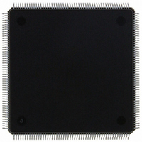
MCF5307AI90B Freescale Semiconductor, MCF5307AI90B Datasheet - Page 81

MCF5307AI90B
Manufacturer Part Number
MCF5307AI90B
Description
IC MPU 32BIT COLDF 90MHZ 208FQFP
Manufacturer
Freescale Semiconductor
Series
MCF530xr
Datasheets
1.MCF5307AI66B.pdf
(484 pages)
2.MCF5307AI66B.pdf
(16 pages)
3.MCF5307AI66B.pdf
(2 pages)
Specifications of MCF5307AI90B
Core Processor
Coldfire V3
Core Size
32-Bit
Speed
90MHz
Connectivity
EBI/EMI, I²C, UART/USART
Peripherals
DMA, POR, WDT
Number Of I /o
16
Program Memory Type
ROMless
Ram Size
4K x 8
Voltage - Supply (vcc/vdd)
3 V ~ 3.6 V
Oscillator Type
External
Operating Temperature
0°C ~ 70°C
Package / Case
208-FQFP
Maximum Clock Frequency
90 MHz
Maximum Operating Temperature
+ 105 C
Mounting Style
SMD/SMT
Minimum Operating Temperature
0 C
Family Name
MCF5xxx
Device Core
ColdFire
Device Core Size
32b
Frequency (max)
90MHz
Instruction Set Architecture
RISC
Supply Voltage 1 (typ)
3.3V
Operating Temp Range
0C to 70C
Operating Temperature Classification
Commercial
Mounting
Surface Mount
Pin Count
208
Package Type
FQFP
Program Memory Size
8KB
Cpu Speed
90MHz
Embedded Interface Type
I2C, UART
Digital Ic Case Style
FQFP
No. Of Pins
208
Supply Voltage Range
3V To 3.6V
Rohs Compliant
Yes
Lead Free Status / RoHS Status
Lead free / RoHS Compliant
Eeprom Size
-
Program Memory Size
-
Data Converters
-
Lead Free Status / Rohs Status
Lead free / RoHS Compliant
Available stocks
Company
Part Number
Manufacturer
Quantity
Price
Company:
Part Number:
MCF5307AI90B
Manufacturer:
FREESCAL
Quantity:
153
Company:
Part Number:
MCF5307AI90B
Manufacturer:
Freescale Semiconductor
Quantity:
10 000
Part Number:
MCF5307AI90B
Manufacturer:
FREESCALE
Quantity:
20 000
- Current page: 81 of 484
- Download datasheet (6Mb)
2.7.1 MOVE Instruction Execution Times
The execution times for the MOVE.{B,W,L} instructions are shown in the next tables.
Table 2-12 shows the timing for the other generic move operations.
ET with {<ea> = (d16,PC)} equals ET with {<ea> = (d16,An)}
ET with {<ea> = (d8,PC,Xi*SF)} equals ET with {<ea> = (d8,An,Xi*SF)}
•
• All operand data accesses are assumed to be aligned on the same byte boundary as
1
certain hardware resources within the processor are marked as “busy” for two clock
cycles after the final DSOC cycle of the store instruction. If a subsequent store
instruction is encountered within this two-cycle window, it is stalled until the
resource again becomes available. Thus, the maximum pipeline stall involving
consecutive store operations is two cycles.
conditions. Thus, timing details in this section assume an infinite zero-wait state
memory attached to the core.
the operand size:
— 16-bit operands aligned on 0-modulo-2 addresses
— 32-bit operands aligned on 0-modulo-4 addresses
Operands that do not meet these guidelines are misaligned. Table 2-9 shows how the
core decomposes a misaligned operand reference into a series of aligned accesses.
Each timing entry is presented as C(r/w), described as follows:
C is the number of processor clock cycles, including all applicable operand fetches and writes, as
well as all internal core cycles required to complete the instruction execution.
r/w is the number of operand reads (r) and writes (w) required by the instruction. An operation
performing a read-modify write function is denoted as (1/1).
The OEP can complete all memory accesses without memory causing any stall
A[1:0]
10
x1
x1
For all tables in this chapter, the execution time of any
instruction using the PC-relative effective addressing modes is
equivalent to the time using comparable An-relative mode.
The nomenclature “(xxx).wl” refers to both forms of absolute
addressing, (xxx).w and (xxx).l.
Table 2-9. Misaligned Operand References
Freescale Semiconductor, Inc.
For More Information On This Product,
Word
Long
Long
Size
Chapter 2. ColdFire Core
Go to: www.freescale.com
Byte, Byte
Byte, Word, Byte
Word, Word
NOTE:
Bus Operations
2(1/0) if read
1(0/1) if write
3(2/0) if read
2(0/2) if write
2(1/0) if read
1(0/1) if write
Additional C(R/W)
Instruction Timing
1
2-41
Related parts for MCF5307AI90B
Image
Part Number
Description
Manufacturer
Datasheet
Request
R
Part Number:
Description:
Manufacturer:
Freescale Semiconductor, Inc
Datasheet:
Part Number:
Description:
Mcf5307 Coldfire Integrated Microprocessor User
Manufacturer:
Freescale Semiconductor, Inc
Datasheet:
Part Number:
Description:
Manufacturer:
Freescale Semiconductor, Inc
Datasheet:
Part Number:
Description:
Manufacturer:
Freescale Semiconductor, Inc
Datasheet:
Part Number:
Description:
Manufacturer:
Freescale Semiconductor, Inc
Datasheet:
Part Number:
Description:
Manufacturer:
Freescale Semiconductor, Inc
Datasheet:
Part Number:
Description:
Manufacturer:
Freescale Semiconductor, Inc
Datasheet:
Part Number:
Description:
Manufacturer:
Freescale Semiconductor, Inc
Datasheet:
Part Number:
Description:
Manufacturer:
Freescale Semiconductor, Inc
Datasheet:
Part Number:
Description:
Manufacturer:
Freescale Semiconductor, Inc
Datasheet:
Part Number:
Description:
Manufacturer:
Freescale Semiconductor, Inc
Datasheet:
Part Number:
Description:
Manufacturer:
Freescale Semiconductor, Inc
Datasheet:
Part Number:
Description:
Manufacturer:
Freescale Semiconductor, Inc
Datasheet:
Part Number:
Description:
Manufacturer:
Freescale Semiconductor, Inc
Datasheet:
Part Number:
Description:
Manufacturer:
Freescale Semiconductor, Inc
Datasheet:


