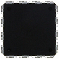
MCF5307AI90B Freescale Semiconductor, MCF5307AI90B Datasheet - Page 197

MCF5307AI90B
Manufacturer Part Number
MCF5307AI90B
Description
IC MPU 32BIT COLDF 90MHZ 208FQFP
Manufacturer
Freescale Semiconductor
Series
MCF530xr
Datasheets
1.MCF5307AI66B.pdf
(484 pages)
2.MCF5307AI66B.pdf
(16 pages)
3.MCF5307AI66B.pdf
(2 pages)
Specifications of MCF5307AI90B
Core Processor
Coldfire V3
Core Size
32-Bit
Speed
90MHz
Connectivity
EBI/EMI, I²C, UART/USART
Peripherals
DMA, POR, WDT
Number Of I /o
16
Program Memory Type
ROMless
Ram Size
4K x 8
Voltage - Supply (vcc/vdd)
3 V ~ 3.6 V
Oscillator Type
External
Operating Temperature
0°C ~ 70°C
Package / Case
208-FQFP
Maximum Clock Frequency
90 MHz
Maximum Operating Temperature
+ 105 C
Mounting Style
SMD/SMT
Minimum Operating Temperature
0 C
Family Name
MCF5xxx
Device Core
ColdFire
Device Core Size
32b
Frequency (max)
90MHz
Instruction Set Architecture
RISC
Supply Voltage 1 (typ)
3.3V
Operating Temp Range
0C to 70C
Operating Temperature Classification
Commercial
Mounting
Surface Mount
Pin Count
208
Package Type
FQFP
Program Memory Size
8KB
Cpu Speed
90MHz
Embedded Interface Type
I2C, UART
Digital Ic Case Style
FQFP
No. Of Pins
208
Supply Voltage Range
3V To 3.6V
Rohs Compliant
Yes
Lead Free Status / RoHS Status
Lead free / RoHS Compliant
Eeprom Size
-
Program Memory Size
-
Data Converters
-
Lead Free Status / Rohs Status
Lead free / RoHS Compliant
Available stocks
Company
Part Number
Manufacturer
Quantity
Price
Company:
Part Number:
MCF5307AI90B
Manufacturer:
FREESCAL
Quantity:
153
Company:
Part Number:
MCF5307AI90B
Manufacturer:
Freescale Semiconductor
Quantity:
10 000
Part Number:
MCF5307AI90B
Manufacturer:
FREESCALE
Quantity:
20 000
- Current page: 197 of 484
- Download datasheet (6Mb)
Chapter 7
Phase-Locked Loop (PLL)
This chapter describes configuration and operation of the phase-locked loop (PLL) module.
It describes in detail the registers and signals that support the PLL implementation.
7.1 Overview
The basic features of the MCF5307 PLL implementation are as follows:
The PLL module has the following three modes of operation:
Figure 7-1 shows the frequency relationships of PLL module clock signals.
z
• The PLL locks to the clock input (CLKIN) frequency. It provides a processor clock
• A buffered processor status clock (PSTCLK) is equal to the PCLK frequency, as
• Reset mode—In reset mode, the core/bus frequency ratio and other configuration
• Normal mode—During normal operations, the divide ratio is programmed at reset
• Reduced-power mode—In reduced-power mode, the high-speed processor core
(PCLK) that is twice the input clock frequency and a programmable system bus
clock output (BCLKO) that is 1/2, 1/3, or 1/4 the PCLK frequency.
indicated in Figure 7-1. This signal is made available for system development.
information is sampled. At reset, the PLL asserts the reset out signal, RSTO.
and is clock-multiplied to provide a maximum frequency of 90 MHz
clocks are turned off without losing the register contents so that the system can be
reenabled by an unmasked interrupt or reset.
DIVIDE[1:0]
FREQ[1:0]
CLKIN
RSTI
Freescale Semiconductor, Inc.
Figure 7-1. PLL Module Block Diagram
For More Information On This Product,
Chapter 7. Phase-Locked Loop (PLL)
CLKIN X 4
PLL
Go to: www.freescale.com
Divide
by 2
Divide by 2,
3, or 4
RSTO
PCLK
PSTCLK
BCLKO
7-1
Related parts for MCF5307AI90B
Image
Part Number
Description
Manufacturer
Datasheet
Request
R
Part Number:
Description:
Manufacturer:
Freescale Semiconductor, Inc
Datasheet:
Part Number:
Description:
Mcf5307 Coldfire Integrated Microprocessor User
Manufacturer:
Freescale Semiconductor, Inc
Datasheet:
Part Number:
Description:
Manufacturer:
Freescale Semiconductor, Inc
Datasheet:
Part Number:
Description:
Manufacturer:
Freescale Semiconductor, Inc
Datasheet:
Part Number:
Description:
Manufacturer:
Freescale Semiconductor, Inc
Datasheet:
Part Number:
Description:
Manufacturer:
Freescale Semiconductor, Inc
Datasheet:
Part Number:
Description:
Manufacturer:
Freescale Semiconductor, Inc
Datasheet:
Part Number:
Description:
Manufacturer:
Freescale Semiconductor, Inc
Datasheet:
Part Number:
Description:
Manufacturer:
Freescale Semiconductor, Inc
Datasheet:
Part Number:
Description:
Manufacturer:
Freescale Semiconductor, Inc
Datasheet:
Part Number:
Description:
Manufacturer:
Freescale Semiconductor, Inc
Datasheet:
Part Number:
Description:
Manufacturer:
Freescale Semiconductor, Inc
Datasheet:
Part Number:
Description:
Manufacturer:
Freescale Semiconductor, Inc
Datasheet:
Part Number:
Description:
Manufacturer:
Freescale Semiconductor, Inc
Datasheet:
Part Number:
Description:
Manufacturer:
Freescale Semiconductor, Inc
Datasheet:


