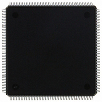
MCF5307AI90B Freescale Semiconductor, MCF5307AI90B Datasheet - Page 410

MCF5307AI90B
Manufacturer Part Number
MCF5307AI90B
Description
IC MPU 32BIT COLDF 90MHZ 208FQFP
Manufacturer
Freescale Semiconductor
Series
MCF530xr
Datasheets
1.MCF5307AI66B.pdf
(484 pages)
2.MCF5307AI66B.pdf
(16 pages)
3.MCF5307AI66B.pdf
(2 pages)
Specifications of MCF5307AI90B
Core Processor
Coldfire V3
Core Size
32-Bit
Speed
90MHz
Connectivity
EBI/EMI, I²C, UART/USART
Peripherals
DMA, POR, WDT
Number Of I /o
16
Program Memory Type
ROMless
Ram Size
4K x 8
Voltage - Supply (vcc/vdd)
3 V ~ 3.6 V
Oscillator Type
External
Operating Temperature
0°C ~ 70°C
Package / Case
208-FQFP
Maximum Clock Frequency
90 MHz
Maximum Operating Temperature
+ 105 C
Mounting Style
SMD/SMT
Minimum Operating Temperature
0 C
Family Name
MCF5xxx
Device Core
ColdFire
Device Core Size
32b
Frequency (max)
90MHz
Instruction Set Architecture
RISC
Supply Voltage 1 (typ)
3.3V
Operating Temp Range
0C to 70C
Operating Temperature Classification
Commercial
Mounting
Surface Mount
Pin Count
208
Package Type
FQFP
Program Memory Size
8KB
Cpu Speed
90MHz
Embedded Interface Type
I2C, UART
Digital Ic Case Style
FQFP
No. Of Pins
208
Supply Voltage Range
3V To 3.6V
Rohs Compliant
Yes
Lead Free Status / RoHS Status
Lead free / RoHS Compliant
Eeprom Size
-
Program Memory Size
-
Data Converters
-
Lead Free Status / Rohs Status
Lead free / RoHS Compliant
Available stocks
Company
Part Number
Manufacturer
Quantity
Price
Company:
Part Number:
MCF5307AI90B
Manufacturer:
FREESCAL
Quantity:
153
Company:
Part Number:
MCF5307AI90B
Manufacturer:
Freescale Semiconductor
Quantity:
10 000
Part Number:
MCF5307AI90B
Manufacturer:
FREESCALE
Quantity:
20 000
- Current page: 410 of 484
- Download datasheet (6Mb)
SIZ[1:0], TM[2:0]
General Operation of External Master Transfers
Note the following regarding external master accesses:
External master transfers that use the MCF5307 to drive memory control signals and TA
are like normal MCF5307 transfers. Figure 18-24 shows timing for basic back-to-back bus
cycles during an external master transfer.
R/W is asserted high for reads and low for writes; otherwise, the transfers are the same. In
Figure 18-24, the MCF5307 chip select’s internal transfer acknowledge is enabled and the
MCF5307 drives TA as an output after a programmed number of wait states.
18-22
A[31:0], TT[1:0]
• For the MCF5307 to assert a CSx during external master accesses, CSMRn[AM]
• To enable DRAM control signals during external master accesses, DCMRn[AM]
• During external master bus cycles, either TS or AS (but not both) should be driven
HOLDREQ
BE/BWE
1
2
BG, BD
This signal is driven by the processor for an external master transfer.
Depending on programming, these signals may or may not be driven by the processor.
BCLKO
D[31:0]
must be set. External master hits use the corresponding CSCRn settings for
auto-acknowledge, byte enables, and wait states. See Section 10.4.1.3, “Chip-Select
Control Registers (CSCR0–CSCR7).”
must be set.
to the MCF5307. Driving both during a bus cycle causes indeterminate results.
CS
BR
R/W
TA
TIP
AS
TS
1
1
1
2
2
Figure 18-24. Basic No-Wait-State External Master Access
C1
Freescale Semiconductor, Inc.
C2
For More Information On This Product,
C3
Go to: www.freescale.com
MCF5307 User’s Manual
C4
C5
External Master
C6
C7
C8
C9
C10
C11
Related parts for MCF5307AI90B
Image
Part Number
Description
Manufacturer
Datasheet
Request
R
Part Number:
Description:
Manufacturer:
Freescale Semiconductor, Inc
Datasheet:
Part Number:
Description:
Mcf5307 Coldfire Integrated Microprocessor User
Manufacturer:
Freescale Semiconductor, Inc
Datasheet:
Part Number:
Description:
Manufacturer:
Freescale Semiconductor, Inc
Datasheet:
Part Number:
Description:
Manufacturer:
Freescale Semiconductor, Inc
Datasheet:
Part Number:
Description:
Manufacturer:
Freescale Semiconductor, Inc
Datasheet:
Part Number:
Description:
Manufacturer:
Freescale Semiconductor, Inc
Datasheet:
Part Number:
Description:
Manufacturer:
Freescale Semiconductor, Inc
Datasheet:
Part Number:
Description:
Manufacturer:
Freescale Semiconductor, Inc
Datasheet:
Part Number:
Description:
Manufacturer:
Freescale Semiconductor, Inc
Datasheet:
Part Number:
Description:
Manufacturer:
Freescale Semiconductor, Inc
Datasheet:
Part Number:
Description:
Manufacturer:
Freescale Semiconductor, Inc
Datasheet:
Part Number:
Description:
Manufacturer:
Freescale Semiconductor, Inc
Datasheet:
Part Number:
Description:
Manufacturer:
Freescale Semiconductor, Inc
Datasheet:
Part Number:
Description:
Manufacturer:
Freescale Semiconductor, Inc
Datasheet:
Part Number:
Description:
Manufacturer:
Freescale Semiconductor, Inc
Datasheet:


