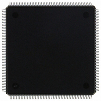
MCF5307AI90B Freescale Semiconductor, MCF5307AI90B Datasheet - Page 392

MCF5307AI90B
Manufacturer Part Number
MCF5307AI90B
Description
IC MPU 32BIT COLDF 90MHZ 208FQFP
Manufacturer
Freescale Semiconductor
Series
MCF530xr
Datasheets
1.MCF5307AI66B.pdf
(484 pages)
2.MCF5307AI66B.pdf
(16 pages)
3.MCF5307AI66B.pdf
(2 pages)
Specifications of MCF5307AI90B
Core Processor
Coldfire V3
Core Size
32-Bit
Speed
90MHz
Connectivity
EBI/EMI, I²C, UART/USART
Peripherals
DMA, POR, WDT
Number Of I /o
16
Program Memory Type
ROMless
Ram Size
4K x 8
Voltage - Supply (vcc/vdd)
3 V ~ 3.6 V
Oscillator Type
External
Operating Temperature
0°C ~ 70°C
Package / Case
208-FQFP
Maximum Clock Frequency
90 MHz
Maximum Operating Temperature
+ 105 C
Mounting Style
SMD/SMT
Minimum Operating Temperature
0 C
Family Name
MCF5xxx
Device Core
ColdFire
Device Core Size
32b
Frequency (max)
90MHz
Instruction Set Architecture
RISC
Supply Voltage 1 (typ)
3.3V
Operating Temp Range
0C to 70C
Operating Temperature Classification
Commercial
Mounting
Surface Mount
Pin Count
208
Package Type
FQFP
Program Memory Size
8KB
Cpu Speed
90MHz
Embedded Interface Type
I2C, UART
Digital Ic Case Style
FQFP
No. Of Pins
208
Supply Voltage Range
3V To 3.6V
Rohs Compliant
Yes
Lead Free Status / RoHS Status
Lead free / RoHS Compliant
Eeprom Size
-
Program Memory Size
-
Data Converters
-
Lead Free Status / Rohs Status
Lead free / RoHS Compliant
Available stocks
Company
Part Number
Manufacturer
Quantity
Price
Company:
Part Number:
MCF5307AI90B
Manufacturer:
FREESCAL
Quantity:
153
Company:
Part Number:
MCF5307AI90B
Manufacturer:
Freescale Semiconductor
Quantity:
10 000
Part Number:
MCF5307AI90B
Manufacturer:
FREESCALE
Quantity:
20 000
- Current page: 392 of 484
- Download datasheet (6Mb)
Data Transfer Operation
The timing relationships between BCLKOchip select (CS[7:0]), byte enable/byte write
enables (BE/BWE[3:0]), and output enable (OE) are similar to their relationships with
address strobe (AS) in that all transitions occur during the low phase of BCLKO. However,
as shown in Figure 18-3, differences in on-chip signal routing and external loading may
prevent signals from asserting simultaneously.
18.4.1 Bus Cycle Execution
When a bus cycle is initiated, the MCF5307 first compares its address with the base address
and mask configurations programmed for chip selects 0–7 (CSCR0–CSCR7) and for
DRAM blocks 0 and 1 address and control registers (DACR0 and DACR1). If the driven
address matches a programmed chip select or DRAM block, the appropriate chip select is
asserted or the DRAM block is selected using the specifications programmed in the
respective configuration register. Otherwise, the following occurs:
18-4
• If the address and attributes do not match in CSCR or DACR, the MCF5307 runs an
• If an address and attribute match in multiple CSCRs, the matching chip-select
• If an address and attribute match both DACRs or a DACR and a CSCR, the operation
external burst-inhibited bus cycle with a default of external termination on a 32-bit
port.
signals are driven; however, the MCF5307 runs an external burst-inhibited bus cycle
with external termination on a 32-bit port.
is undefined.
BE/BWE[3:0]
Figure 18-2. Connections for External Memory Port Sizes
Figure 18-3. Chip-Select Module Output Timing Diagram
BCLKO
CS[7:0]
AS, OE
Byte Enable
32-Bit Port
16-Bit Port
Processor
Freescale Semiconductor, Inc.
8-Bit Port
Data Bus
External
Memory
Memory
Memory
For More Information On This Product,
Go to: www.freescale.com
MCF5307 User’s Manual
D[31:24]
Byte 0
Byte 0
Byte 2
Byte 0
Byte 1
Byte 2
Byte 3
BE0
D[23:16]
Byte 1
Byte 1
Byte 3
BE1
indeterminate values
Driven with
indeterminate values
D[15:8]
Byte 2
BE2
Driven with
Byte 3
D[7:0]
BE3
Related parts for MCF5307AI90B
Image
Part Number
Description
Manufacturer
Datasheet
Request
R
Part Number:
Description:
Manufacturer:
Freescale Semiconductor, Inc
Datasheet:
Part Number:
Description:
Mcf5307 Coldfire Integrated Microprocessor User
Manufacturer:
Freescale Semiconductor, Inc
Datasheet:
Part Number:
Description:
Manufacturer:
Freescale Semiconductor, Inc
Datasheet:
Part Number:
Description:
Manufacturer:
Freescale Semiconductor, Inc
Datasheet:
Part Number:
Description:
Manufacturer:
Freescale Semiconductor, Inc
Datasheet:
Part Number:
Description:
Manufacturer:
Freescale Semiconductor, Inc
Datasheet:
Part Number:
Description:
Manufacturer:
Freescale Semiconductor, Inc
Datasheet:
Part Number:
Description:
Manufacturer:
Freescale Semiconductor, Inc
Datasheet:
Part Number:
Description:
Manufacturer:
Freescale Semiconductor, Inc
Datasheet:
Part Number:
Description:
Manufacturer:
Freescale Semiconductor, Inc
Datasheet:
Part Number:
Description:
Manufacturer:
Freescale Semiconductor, Inc
Datasheet:
Part Number:
Description:
Manufacturer:
Freescale Semiconductor, Inc
Datasheet:
Part Number:
Description:
Manufacturer:
Freescale Semiconductor, Inc
Datasheet:
Part Number:
Description:
Manufacturer:
Freescale Semiconductor, Inc
Datasheet:
Part Number:
Description:
Manufacturer:
Freescale Semiconductor, Inc
Datasheet:


