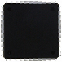
MCF5307AI90B Freescale Semiconductor, MCF5307AI90B Datasheet - Page 434

MCF5307AI90B
Manufacturer Part Number
MCF5307AI90B
Description
IC MPU 32BIT COLDF 90MHZ 208FQFP
Manufacturer
Freescale Semiconductor
Series
MCF530xr
Datasheets
1.MCF5307AI66B.pdf
(484 pages)
2.MCF5307AI66B.pdf
(16 pages)
3.MCF5307AI66B.pdf
(2 pages)
Specifications of MCF5307AI90B
Core Processor
Coldfire V3
Core Size
32-Bit
Speed
90MHz
Connectivity
EBI/EMI, I²C, UART/USART
Peripherals
DMA, POR, WDT
Number Of I /o
16
Program Memory Type
ROMless
Ram Size
4K x 8
Voltage - Supply (vcc/vdd)
3 V ~ 3.6 V
Oscillator Type
External
Operating Temperature
0°C ~ 70°C
Package / Case
208-FQFP
Maximum Clock Frequency
90 MHz
Maximum Operating Temperature
+ 105 C
Mounting Style
SMD/SMT
Minimum Operating Temperature
0 C
Family Name
MCF5xxx
Device Core
ColdFire
Device Core Size
32b
Frequency (max)
90MHz
Instruction Set Architecture
RISC
Supply Voltage 1 (typ)
3.3V
Operating Temp Range
0C to 70C
Operating Temperature Classification
Commercial
Mounting
Surface Mount
Pin Count
208
Package Type
FQFP
Program Memory Size
8KB
Cpu Speed
90MHz
Embedded Interface Type
I2C, UART
Digital Ic Case Style
FQFP
No. Of Pins
208
Supply Voltage Range
3V To 3.6V
Rohs Compliant
Yes
Lead Free Status / RoHS Status
Lead free / RoHS Compliant
Eeprom Size
-
Program Memory Size
-
Data Converters
-
Lead Free Status / Rohs Status
Lead free / RoHS Compliant
Available stocks
Company
Part Number
Manufacturer
Quantity
Price
Company:
Part Number:
MCF5307AI90B
Manufacturer:
FREESCAL
Quantity:
153
Company:
Part Number:
MCF5307AI90B
Manufacturer:
Freescale Semiconductor
Quantity:
10 000
Part Number:
MCF5307AI90B
Manufacturer:
FREESCALE
Quantity:
20 000
- Current page: 434 of 484
- Download datasheet (6Mb)
Restrictions
19.4.4 JTAG Bypass Register
The IEEE Standard 1149.1-compliant bypass register creates a single-bit shift register path
from TDI to the bypass register to TDO when the BYPASS instruction is selected.
19.5 Restrictions
Test logic design is static, so TCK can be stopped in high or low state with no data loss.
However, system logic uses a different system clock not internally synchronized to TCK.
Operation mixing 1149.1 test logic with system functional logic that uses both clocks must
coordinate and synchronize these clocks externally to the MCF5307.
19-10
101
102
103
104
105
106
107
108
109
110
111
112
113
114
115
116
117
118
119
Bit
Cell Type
O.Pin
O.Pin
O.Pin
O.Pin
O.Pin
O.Pin
O.Pin
O.Pin
O.Pin
O.Pin
O.Pin
I.Pin
I.Pin
I.Pin
I.Pin
I.Pin
I.Pin
I.Pin
I.Pin
D26
D26
D27
D27
D28
D28
D29
D29
D30
D30
D31
D31
SDA
SDA
SCL
SCL
BE3
BE2
BE1
Pin Cell
Table 19-4. Boundary-Scan Bit Definitions
Freescale Semiconductor, Inc.
For More Information On This Product,
Pin Type
Go to: www.freescale.com
MCF5307 User’s Manual
OD
OD
I/O
I/O
I/O
I/O
I/O
I/O
I/O
I/O
I/O
I/O
I/O
I/O
O
O
O
I
I
221
222
223
224
225
226
227
228
229
230
231
232
233
234
235
236
237
238
Bit
Cell Type
O.Pin
O.Pin
O.Pin
O.Pin
O.Pin
O.Pin
O.Pin
O.Pin
O.Pin
I.Pin
I.Pin
I.Pin
I.Pin
I.Pin
I.Pin
I.Pin
I.Pin
I.Pin
A8
A8
A7
A7
A6
A6
A5
A5
A4
A4
A3
A3
A2
A2
A1
A1
A0
A0
Pin Cell
Pin Type
I/O
I/O
I/O
I/O
I/O
I/O
I/O
I/O
I/O
I/O
I/O
I/O
I/O
I/O
I/O
I/O
I/O
I/O
Related parts for MCF5307AI90B
Image
Part Number
Description
Manufacturer
Datasheet
Request
R
Part Number:
Description:
Manufacturer:
Freescale Semiconductor, Inc
Datasheet:
Part Number:
Description:
Mcf5307 Coldfire Integrated Microprocessor User
Manufacturer:
Freescale Semiconductor, Inc
Datasheet:
Part Number:
Description:
Manufacturer:
Freescale Semiconductor, Inc
Datasheet:
Part Number:
Description:
Manufacturer:
Freescale Semiconductor, Inc
Datasheet:
Part Number:
Description:
Manufacturer:
Freescale Semiconductor, Inc
Datasheet:
Part Number:
Description:
Manufacturer:
Freescale Semiconductor, Inc
Datasheet:
Part Number:
Description:
Manufacturer:
Freescale Semiconductor, Inc
Datasheet:
Part Number:
Description:
Manufacturer:
Freescale Semiconductor, Inc
Datasheet:
Part Number:
Description:
Manufacturer:
Freescale Semiconductor, Inc
Datasheet:
Part Number:
Description:
Manufacturer:
Freescale Semiconductor, Inc
Datasheet:
Part Number:
Description:
Manufacturer:
Freescale Semiconductor, Inc
Datasheet:
Part Number:
Description:
Manufacturer:
Freescale Semiconductor, Inc
Datasheet:
Part Number:
Description:
Manufacturer:
Freescale Semiconductor, Inc
Datasheet:
Part Number:
Description:
Manufacturer:
Freescale Semiconductor, Inc
Datasheet:
Part Number:
Description:
Manufacturer:
Freescale Semiconductor, Inc
Datasheet:


