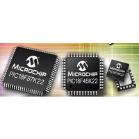
PIC18F46K22-I/MV Microchip Technology, PIC18F46K22-I/MV Datasheet - Page 138

PIC18F46K22-I/MV
Manufacturer Part Number
PIC18F46K22-I/MV
Description
64KB, Flash, 3968bytes-RAM,8-bit Family,nanoWatt XLP 40 UQFN 5x5x0.5mm TUBE
Manufacturer
Microchip Technology
Series
PIC® XLP™ 18Fr
Datasheet
1.PIC18F26J13-ISS.pdf
(496 pages)
Specifications of PIC18F46K22-I/MV
Core Processor
PIC
Core Size
8-Bit
Speed
64MHz
Connectivity
I²C, SPI, UART/USART
Peripherals
Brown-out Detect/Reset, HLVD, POR, PWM, WDT
Number Of I /o
35
Program Memory Size
64KB (32K x 16)
Program Memory Type
FLASH
Eeprom Size
1K x 8
Ram Size
3.8K x 8
Voltage - Supply (vcc/vdd)
1.8 V ~ 5.5 V
Data Converters
A/D 30x10b
Oscillator Type
Internal
Operating Temperature
-40°C ~ 85°C
Package / Case
40-UFQFN Exposed Pad
Processor Series
PIC18F
Core
PIC
Data Bus Width
8 bit
Data Ram Size
4 KB
Number Of Programmable I/os
36
Number Of Timers
3 x 8-bit. 4 x 16-bit
Operating Supply Voltage
1.8 V to 5.5 V
Mounting Style
SMD/SMT
Lead Free Status / RoHS Status
Lead free / RoHS Compliant
Lead Free Status / RoHS Status
Lead free / RoHS Compliant
- Current page: 138 of 496
- Download datasheet (5Mb)
PIC18(L)F2X/4XK22
10.2
PORTB is an 8-bit wide, bidirectional port. The
corresponding data direction register is TRISB. Setting
a TRISB bit (= 1) will make the corresponding PORTB
pin an input (i.e., disable the output driver). Clearing a
TRISB bit (= 0) will make the corresponding PORTB
pin an output (i.e., enable the output driver and put the
contents of the output latch on the selected pin).
The Data Latch register (LATB) is also memory
mapped. Read-modify-write operations on the LATB
register read and write the latched output value for
PORTB.
EXAMPLE 10-2:
10.2.1
Each PORTB pin is multiplexed with other functions.
The pins, their combined functions and their output
priorities are briefly described here. For additional
information, refer to the appropriate section in this data
sheet.
When multiple outputs are enabled, the actual pin
control goes to the peripheral with the higher priority.
Table 10-4
highest to the lowest priority.
Analog input functions, such as ADC, comparator and
SR Latch inputs, are not shown in the priority lists.
These inputs are active when the I/O pin is set for
Analog mode using the ANSELx registers. Digital
output functions may control the pin when it is in Analog
mode with the priority shown below.
DS41412D-page 138
MOVLB
CLRF
CLRF
MOVLW
MOVWF
MOVLW
MOVWF
PORTB Registers
0xF
PORTB
LATB
0F0h
ANSELB ; Enable RB<3:0> for
0CFh
TRISB
PORTB OUTPUT PRIORITY
lists the PORTB pin functions from the
; Set BSR for banked SFRs
; Initialize PORTB by
; clearing output
; data latches
; Alternate method
; to clear output
; data latches
; Value for init
; digital input pins
; (not required if config bit
; PBADEN is clear)
; Value used to
; initialize data
; direction
; Set RB<3:0> as inputs
; RB<5:4> as outputs
; RB<7:6> as inputs
INITIALIZING PORTB
Preliminary
10.3
PORTB pins RB<7:4> have an interrupt-on-change
option. All PORTB pins have a weak pull-up option.
10.3.1
Each of the PORTB pins has an individually controlled
weak internal pull-up. When set, each bit of the WPUB
register enables the corresponding pin pull-up. When
cleared, the RBPU bit of the INTCON2 register enables
pull-ups on all pins which also have their corresponding
WPUB bit set. When set, the RBPU bit disables all
weak pull-ups. The weak pull-up is automatically turned
off when the port pin is configured as an output. The
pull-ups are disabled on a Power-on Reset.
10.3.2
Four of the PORTB pins (RB<7:4>) are individually
configurable as interrupt-on-change pins. Control bits
in the IOCB register enable (when set) or disable (when
clear) the interrupt function for each pin.
When set, the RBIE bit of the INTCON register enables
interrupts on
corresponding IOCB bit set. When clear, the RBIE bit
disables all interrupt-on-changes.
Only pins configured as inputs can cause this interrupt
to occur (i.e., any RB<7:4> pin configured as an output
is excluded from the interrupt-on-change comparison).
For enabled interrupt-on-change pins, the values are
compared with the old value latched on the last read of
PORTB. The ‘mismatch’ outputs of the last read are
OR’d together to set the PORTB Change Interrupt flag
bit (RBIF) in the INTCON register.
This interrupt can wake the device from the Sleep
mode, or any of the Idle modes. The user, in the
Interrupt Service Routine, can clear the interrupt in the
following manner:
a)
b)
Note:
Any read or write of PORTB to clear the mis-
match condition (except when PORTB is the
source or destination of a MOVFF instruction).
Execute at least one instruction after reading or
writing PORTB, then clear the flag bit, RBIF.
Additional PORTB Pin Functions
WEAK PULL-UPS
On a Power-on Reset, RB<5:0> are
configured as analog inputs by default and
read as ‘0’; RB<7:6> are configured as
digital inputs.
When the PBADEN Configuration bit is
set to ‘1’, RB<5:0> will alternatively be
configured as digital inputs on POR.
INTERRUPT-ON-CHANGE
all
pins
2010 Microchip Technology Inc.
which
also
have
their
Related parts for PIC18F46K22-I/MV
Image
Part Number
Description
Manufacturer
Datasheet
Request
R

Part Number:
Description:
Manufacturer:
Microchip Technology Inc.
Datasheet:

Part Number:
Description:
Manufacturer:
Microchip Technology Inc.
Datasheet:

Part Number:
Description:
Manufacturer:
Microchip Technology Inc.
Datasheet:

Part Number:
Description:
Manufacturer:
Microchip Technology Inc.
Datasheet:

Part Number:
Description:
Manufacturer:
Microchip Technology Inc.
Datasheet:

Part Number:
Description:
Manufacturer:
Microchip Technology Inc.
Datasheet:

Part Number:
Description:
Manufacturer:
Microchip Technology Inc.
Datasheet:

Part Number:
Description:
Manufacturer:
Microchip Technology Inc.
Datasheet:


